A Pre Nvidia GTC Thesis Update
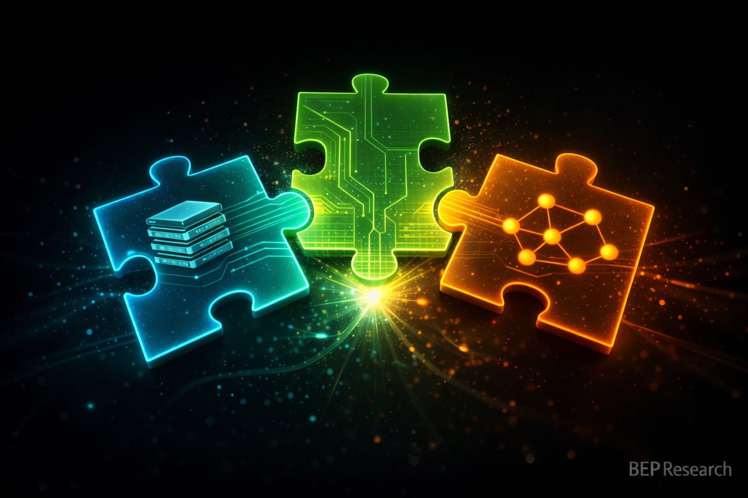
Three Pieces of the Puzzle

Good morning, its Sunday. Pour yourself a cup of coffee, find a quiet spot, and settle in. Weekends are for philosophy and deep thinking without interruption. This one pulls together two months of research into a single frame—and with NVIDIA earnings this Wednesday and GTC three weeks out, the timing matters.
Over the past two months, I’ve published a small book’s worth of analysis across this newsletter building a single argument: the AI inference bottleneck isn’t compute. It’s memory. And the companies solving that bottleneck through co-design—hardware, software, and deployment as a unified system—will capture the next decade of value.
With NVIDIA’s GTC 2026 three weeks away (Jensen’s keynote is March 16 at SAP Center in San Jose), it’s worth mapping exactly where the thesis stands—and what I’ll be watching for.
I’ll be at GTC in person this year, covering Jensen’s keynote and sessions live for BEP Research subscribers. If the thesis meets reality on March 16, you’ll hear about it in real time. (Register for GTC 2026 here — virtual access is free.)
There are three pieces to this puzzle. All three are now in motion.
Piece One: Stacked Memory
The memory wall is real, and it’s getting worse. FLOPS scale roughly 750× every two years while DRAM bandwidth scales only 1.6×. From V100 to H100, NVIDIA’s compute-to-bandwidth ratio doubled from 139:1 to 295:1—making GPUs progressively worse-suited for memory-bound inference workloads.
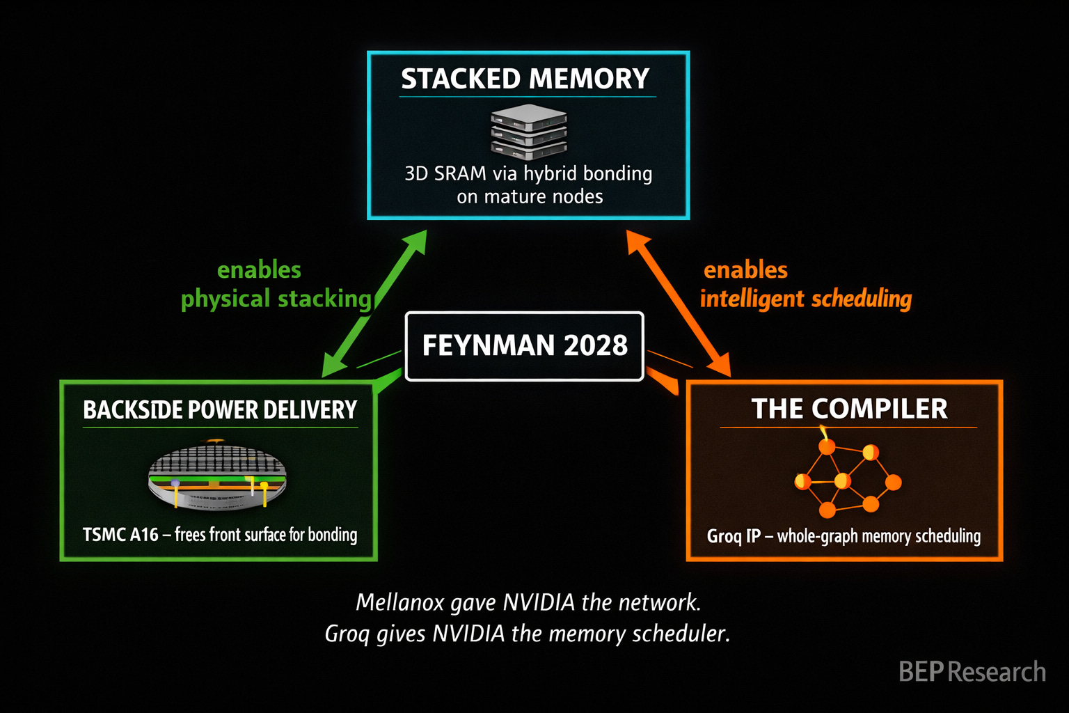
I laid out the full picture in The Memory Wars: NVIDIA’s Feynman architecture (2028) won’t fight SRAM scaling physics. It routes around them. The plan is 3D-stacked SRAM using hybrid bonding on separate, cheaper process nodes—the same principle AMD proved with 3D V-Cache, but applied to inference at datacenter scale.
The economics are converging faster than anyone modeled. In Raja Was Right, I tracked the DRAM/SRAM cost ratio from ~8× at the time of Raja Koduri’s February 2024 warning to roughly 2× today. We blew through his 5× threshold six months ago. The ratio is still compressing. Every HBM price increase accelerates it.
What matters for GTC: any detail on how NVIDIA plans to integrate stacked SRAM into the Rubin or Feynman roadmap. The architecture definition is happening now for products shipping in 2028-2029. If Jensen shows a memory hierarchy diagram that includes a stacked SRAM tier alongside HBM, that’s the hardware confirmation.
Piece Two: Backside Power Delivery
Stacked memory alone doesn’t solve the problem. You need somewhere to put the hybrid bonds.
Traditional chips route both power and data on the front surface. That creates congestion—physical routing nightmares when you try to stack memory dies on top of the compute die. The traces carrying power compete with the traces carrying data for the same limited real estate.
TSMC’s A16 node, with Super Power Rail backside power delivery, changes this equation entirely. Moving power to the back of the wafer frees the front surface for high-density hybrid bonding. That’s what makes 3D SRAM stacking practical without front-side routing nightmares.
As I wrote in The Memory Wars: “Backside power delivery is the key enabler.” NVIDIA is reportedly the first—and initially only—customer for A16. That’s not a coincidence. They need backside power delivery not just for density or power efficiency, but because it’s the prerequisite for making the stacked memory architecture physically work.
This also explains why NVIDIA is skipping TSMC’s baseline N2 entirely. The choice isn’t about transistor density. It’s about what the back of the wafer enables on the front.
What matters for GTC: any mention of A16 timelines or backside power delivery in the context of memory architecture. The packaging roadmap is the real roadmap.
Piece Three: The Compiler
Here’s the piece that most semiconductor analysts miss entirely, and it’s the one I’ve been most focused on since the Groq deal.
You can stack all the memory you want. You can free the front surface with backside power delivery. But without a compiler that knows how to schedule data movement across a heterogeneous memory hierarchy—HBM for capacity, stacked SRAM for speed, system memory for overflow—you’ve built an engine without a transmission.
This is what Groq’s architecture proved in the extreme. Their LPU achieves 276 tokens/sec on Llama 3.3 70B—versus 60-100 on GPUs—not because of faster transistors, but because of a compiler that eliminates memory stalls through static, whole-graph scheduling. Deterministic execution. No cache misses. No memory hierarchy surprises. The compiler knows where every byte lives before the first instruction fires.
In ‘Twas the Night Before Groq, I argued NVIDIA didn’t pay $20 billion for Groq’s chips. They paid for “whole-graph scheduling techniques, deterministic execution models, compiler strategies for inference-first workloads.” The hardware template was interesting. The compiler DNA was essential.
I’ve been thinking about this deal through the acquisition lens, and here’s where I’ll plant a flag: Groq could be as instrumental to NVIDIA as Mellanox was. Mellanox gave NVIDIA the networking fabric that turned individual GPUs into a datacenter-scale compute platform—it was the connective tissue that made NVLink, InfiniBand, and eventually the NVL72 rack architecture possible. Without Mellanox, NVIDIA sells chips. With Mellanox, NVIDIA sells systems. The Groq IP may do the same thing for the memory hierarchy. It gives NVIDIA the compiler intelligence to turn a heterogeneous stack of HBM, stacked SRAM, and system memory into a unified, software-scheduled memory platform. Without Groq’s scheduling insights, the stacked memory architecture is fast but dumb. With them, it becomes a system that knows where every byte should live and when it should move. That’s the difference between selling silicon and selling inference infrastructure.
Now consider what that compiler technology looks like when applied not to Groq’s extreme all-SRAM architecture, but to NVIDIA’s planned hybrid: stacked SRAM on top of a compute die with backside power delivery, surrounded by HBM stacks for capacity, with NVLink connecting multiple packages. The compiler needs to know which data lives where, when to prefetch from HBM into SRAM, how to schedule operations to avoid stalls, and how to partition work across the hierarchy.
That’s not a CUDA extension. That’s a fundamentally new scheduling paradigm—one that borrows heavily from exactly the kind of compiler-driven dataflow that Groq pioneered.
What matters for GTC: any announcement of new compiler infrastructure, scheduling frameworks, or memory management tools for heterogeneous memory hierarchies. This could show up in the CUDA keynote, in TensorRT-LLM updates, or in NVIDIA Dynamo enhancements. If they demo a compiler that can intelligently place and schedule across multiple memory tiers, that’s the software piece clicking into place.
Meanwhile: Taalas and the Inference Desperation Trade
While the three-piece thesis plays out at the architecture level, the market is sending its own signal about just how severe the inference bottleneck has become.
This week, Toronto-based startup Taalas came out of stealth with $219 million in total funding (Quiet Capital, Fidelity, Pierre Lamond) and a provocative claim: 17,000 tokens per second on Llama 3.1 8B. That’s roughly 10× faster than current GPU solutions. No HBM. No liquid cooling. No advanced packaging. Just model weights literally etched into the final two metal layers of a TSMC 6nm chip.
The Twitter hype machine predictably declared NVIDIA dead. Let’s slow down.
Taalas is Groq’s thesis taken to its logical extreme—and it inherits all of Groq’s limitations plus new ones. The model is frozen in silicon. No weight updates. No fine-tuning beyond LoRA adapters. Their HC1 hosts an 8B parameter model on a near-reticle-limit die (~815mm²). Frontier models at 400B-1T parameters would require enormous chip clusters. Their own numbers show DeepSeek R1 requiring a 30-chip configuration. And the aggressive 3-bit quantization introduces quality degradation they openly acknowledge.
Founded by Ljubisa Bajic—who previously co-founded Tenstorrent with Jim Keller and worked at both AMD and NVIDIA—Taalas represents serious engineering talent pursuing extreme specialization. That deserves respect. But the approach has a structural ceiling: every new model version requires a new fabrication run. In a world where frontier models update quarterly, that’s a business model constraint, not just a technical one.
Here’s what actually matters: $219 million in venture capital flowing into inference-specific silicon validates that the bottleneck is real enough and painful enough that sophisticated investors will fund extreme solutions. The inference latency and cost problem is not theoretical. It’s driving capital allocation decisions right now.
But NVIDIA’s answer—Groq’s compiler DNA applied to a flexible, heterogeneous memory architecture with stacked SRAM, HBM, and backside power delivery—aims to capture the same performance gains while retaining the generality that Taalas sacrifices. Taalas validates the problem. The three-piece convergence is the scalable solution.
In ‘Twas the Night Before Groq, I wrote: “You study the extreme to understand the envelope, then you build something practical that captures the lessons.” Taalas is another extreme data point. NVIDIA is building the practical system.
The Numbers Heading Into Earnings
NVIDIA reports Q4 FY2026 earnings on February 26—one week from today, and three weeks before GTC. The fundamental picture heading into the print deserves attention.
TSMC’s CoWoS capacity is now projected to expand to 125,000-145,000 wafer starts per month by the end of CY2026/27, with NVIDIA likely securing an allocation of over 60% in 2027. That’s the supply-side constraint that underpins pricing power. As I detailed in The Packaging Paradox, CoWoS—not transistor node—is the real bottleneck, and NVIDIA’s dominant allocation share means they benefit from both the capacity expansion and the scarcity premium.
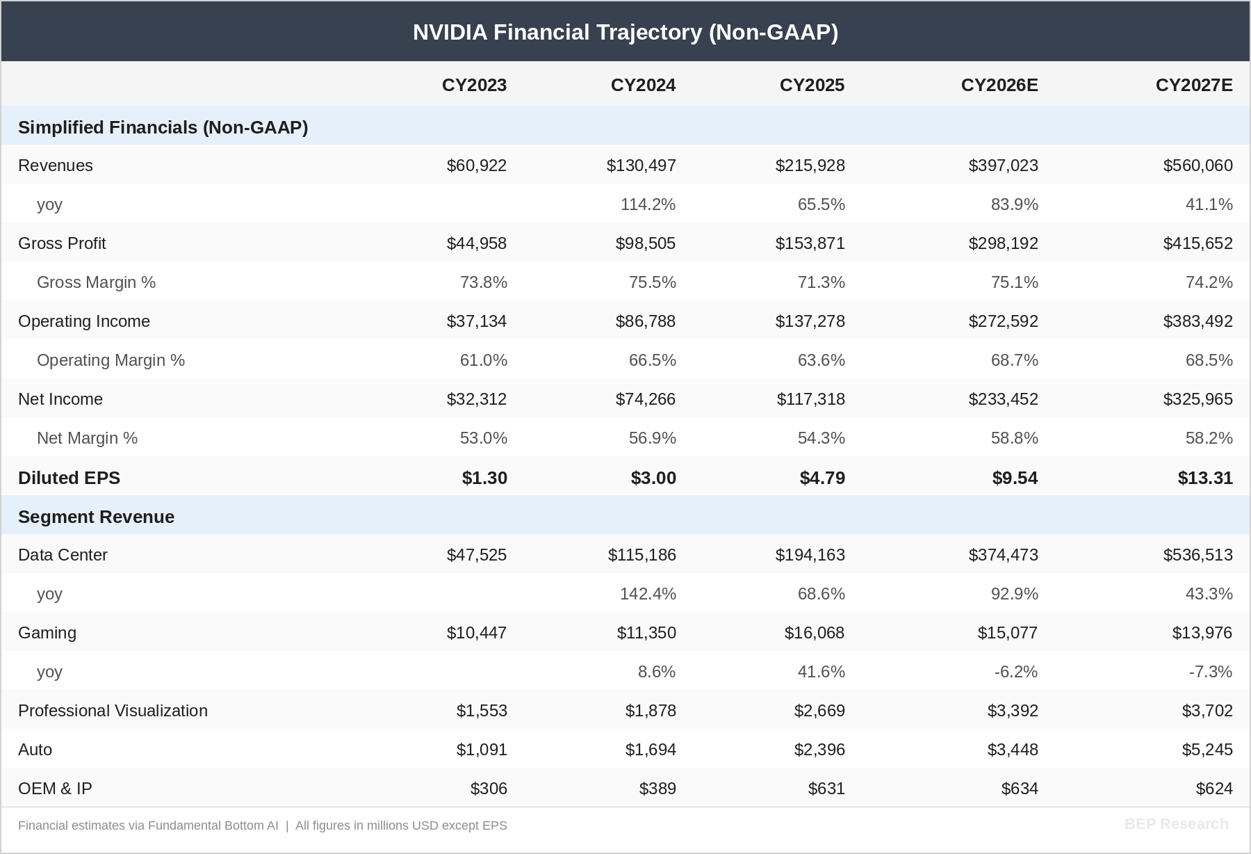
The street models I track closely, including FundaAI’s detailed build, project NVIDIA’s Data Center revenue reaching approximately $537 billion by CY2027, representing roughly 43% year-over-year growth off an estimated $374 billion in CY2026. That trajectory implies total company revenue approaching $560 billion with EPS of approximately $13.30—putting the stock at roughly 14× forward earnings on CY2027 numbers.
Meanwhile, the competitive landscape is quietly shifting in NVIDIA’s favor. On Sunday, I reported on X that Google did not submit a TPU for the upcoming MLPerf Inference v6.0 benchmark. The deadline to submit was Friday, February 13, and results will be published in the coming weeks. NVIDIA dominated MLPerf Inference v5.1 last September, including winning the critically important reasoning model category with DeepSeek-R1—the type of workload where models perform extended chains of thought and multiple computations before responding. Reasoning model usage is accelerating as they deliver significantly more accurate and higher-quality answers than prior architectures.
Google’s absence from MLPerf v6.0 is notable. TPU has historically been a credible benchmark competitor, and choosing not to submit—while NVIDIA continues to set records—suggests either timing issues with Ironwood qualification or a strategic decision to avoid a direct comparison that wouldn’t favor them. Either way, it reinforces NVIDIA’s inference leadership narrative heading into both earnings and GTC.
The key tension: at ~14× CY2027 earnings, NVIDIA is not priced for perfection. It’s priced for deceleration. If the three-piece convergence I’ve outlined—stacked memory, backside power, the compiler—materializes on the Feynman roadmap, the inference revenue opportunity extends well beyond what current models capture. Inference economics improve → inference demand becomes more elastic → the total addressable market expands.
Gross margins tell the competitive moat story. The projection holds margins in the 74-75% range through 2027 despite massive revenue scaling. That’s not a hardware commodity business. That’s stack depth—CUDA, TensorRT-LLM, Dynamo, NVLink—creating the switching costs that sustain pricing power even as capacity expands.
I’ll cover the earnings print in detail for subscribers next week. The number to watch isn’t the Q4 beat—that’s likely priced in. It’s the forward guidance commentary on inference demand, Blackwell ramp trajectory, and any early signals about Rubin allocation.
The Convergence
These three pieces aren’t independent. They’re co-designed—which is exactly what makes the thesis compelling and what makes it hard for competitors to replicate.
Stacked memory needs backside power delivery to be physically viable. Backside power delivery needs stacked memory to justify the premium of A16 over N2. And both need a new compiler paradigm to actually deliver the performance the architecture promises.
This is what Jensen meant at CES when he said “extreme co-design.” The six chips he announced—Vera CPU, Rubin GPU, NVLink 6 Switch, Spectrum-X CPO, ConnectX-9 SuperNIC, BlueField-4 DPU—weren’t designed independently. They were designed as a system. Each silicon decision was informed by how it would interact with every other component.
I covered this in detail in NVIDIA CES 2026: Six Chips, One Platform and NVIDIA’s Inference Stack Depth Strategy. The $30 billion+ in acquisitions and licensing deals since 2024—Mellanox, Run:ai, Deci, Groq, BlueField—maps directly to memory hierarchy layers. Stack depth isn’t a buzzword. It’s an engineering program.
And startups like Taalas—impressive as their engineering is—are actually proving why the co-design approach wins. You can get extraordinary performance from total specialization, but you sacrifice the flexibility that real-world deployment requires. NVIDIA’s bet is that compiler-driven optimization of a heterogeneous memory hierarchy gets you 80% of the specialization benefit with none of the brittleness. If the Groq IP delivers on that promise, it’s the best of both worlds.
And there’s a fourth piece I haven’t discussed yet—optical die-to-die interconnect from ISSCC, which changes how these stacked memory packages talk to each other across the system. I covered the technology stack in my AI Datacenter Optical Interconnect Boom deep dive. A dedicated analysis on how optical die-to-die fits into the Feynman architecture is coming soon.
What I’m Watching at GTC
Jensen’s keynote is Monday, March 16, 11 AM Pacific at the SAP Center. I’ll be in the room. Register here to watch the keynote live or on demand.
Here’s my watch list, in order of signal importance:
Memory architecture details for Rubin Ultra and Feynman. Any mention of stacked SRAM, hybrid bonding for memory dies, or tiered memory hierarchies within a single package. This is the hardware confirmation of the thesis.
Compiler and scheduling announcements. New TensorRT-LLM capabilities for heterogeneous memory, NVIDIA Dynamo enhancements for distributed KV cache, or any new framework for memory-aware scheduling. The software piece is the one most likely to be demo-ready before the silicon ships.
A16 timeline clarity. Any update on when TSMC’s backside power delivery node enters production for NVIDIA. The current expectation is 2027-2028, but acceleration or delays change the entire roadmap.
Inference economics. The January TensorRT-LLM update delivered 2.8× higher token throughput on existing GB200 hardware—pure software gains on the same silicon. If NVIDIA shows another step-function improvement, it validates that compiler optimization is still in early innings.
Groq integration signals. Any mention of deterministic execution, static scheduling, or inference-specific compiler passes that echo Groq’s architecture. The $20 billion deal closes its value loop when the technology shows up in NVIDIA’s shipping stack.
Rubin deployment and demand signals. How the Blackwell-to-Rubin transition is being communicated to customers, and any guidance on allocation, pricing, or delivery timelines that feeds into the CY2027 financial models.
The Investment Frame
For existing BEP Research readers, none of this changes the core positioning I’ve outlined across the co-design series. But the next four weeks—earnings on February 26, then GTC on March 16—will stress-test the thesis in real time.
If NVIDIA confirms the three-piece convergence—stacked memory, backside power delivery, and a new compiler paradigm—it validates the entire analytical arc from The Memory Wall through Raja Was Right. Companies positioned across this convergence (TSMC for packaging, the hybrid bonding equipment suppliers, NVIDIA itself) strengthen. Companies betting purely on HBM scaling without architectural alternatives face growing risk.
If NVIDIA focuses exclusively on Rubin without addressing the 2028+ architecture, it suggests the timeline is longer than expected—which is also valuable information for portfolio positioning.
Either way, the next month is when the thesis meets reality. The pieces are in motion. I’ll be there to see whether they lock together.
Earnings coverage drops next week. GTC coverage will be live from San Jose. Register for GTC and subscribe to make sure you don’t miss either.
What’s Changing
On March 9th, BEP Research moves to paid subscriptions—timed deliberately to NVIDIA’s GTC conference the following week, where I’ll be on the ground. Paid subscribers get exclusive real-time GTC coverage: in-depth analysis of every major announcement, on-the-ground interviews, and breakdowns of what roadmap changes mean for your portfolio. Not recaps. Real analysis, in real time.
After March 9th, the deep work—Co-Design Thesis series, investment frameworks, earnings breakdowns, supply chain deep dives, and all GTC coverage—moves behind the paywall. Free subscribers will still receive post summaries and occasional public pieces.
Early Bird: ~$350/year (13% off) — available now through March 9th only.
→ Lock in the Early Bird rate here
After March 9th, standard pricing applies: $400/year | $45/month | Founding Member: $450/year (permanent recognition + priority access to the institutional tier).
This is premium-priced on purpose. Institutional-quality research without sell-side conflicts, without advertising, without surface-level takes. If one analysis helps you size a position correctly or avoid a bad trade, the subscription pays for itself many times over.
Institutional Access: I’m developing a tier for teams and funds with multi-seat licenses, direct analyst calls, and priority Q&A. If that’s relevant to your team, reply to this email.
The early bird window closes March 9th. See you at GTC.
Related BEP Research
The Memory Wars: Why NVIDIA’s 2028 Architecture Ends the AI Chip Competition
Raja Was Right: The 5× Threshold and the Memory Cost Reckoning
‘Twas the Night Before Groq: NVIDIA’s Surprise Licensing Deal Is Not What You Think
NVIDIA CES 2026: Six Chips, One Platform, and the Extreme Codesign Era
The Packaging Paradox: Why CoWoS—Not 2nm—Is the Real AI Bottleneck
About the Author
Ben Pouladian is a Los Angeles-based tech investor and entrepreneur focused on AI infrastructure, semiconductors, and the power systems enabling the next generation of compute. He was co-founder of Deco Lighting (2005–2019), where he helped build one of the leading commercial LED lighting manufacturers in North America. Ben holds an electrical engineering degree from UC San Diego, where he worked in Professor Fainman’s ultrafast nanoscale optics lab on silicon photonics and micro-ring resonators, and interned at Cymer, the company that manufactures the EUV light sources for ASML’s lithography systems.
He currently serves as Chairman of the Leadership Board at Terasaki Institute for Biomedical Innovation and is a YPO member. His investment research focuses on AI datacenter infrastructure, GPU computing, and the semiconductor supply chain. Long-term NVIDIA investor since 2016.
Follow on Twitter/X: @benitoz | More at benpouladian.com
Disclosure: The author holds positions in NVIDIA and related semiconductor investments. This is not investment advice.
Can’t wait