

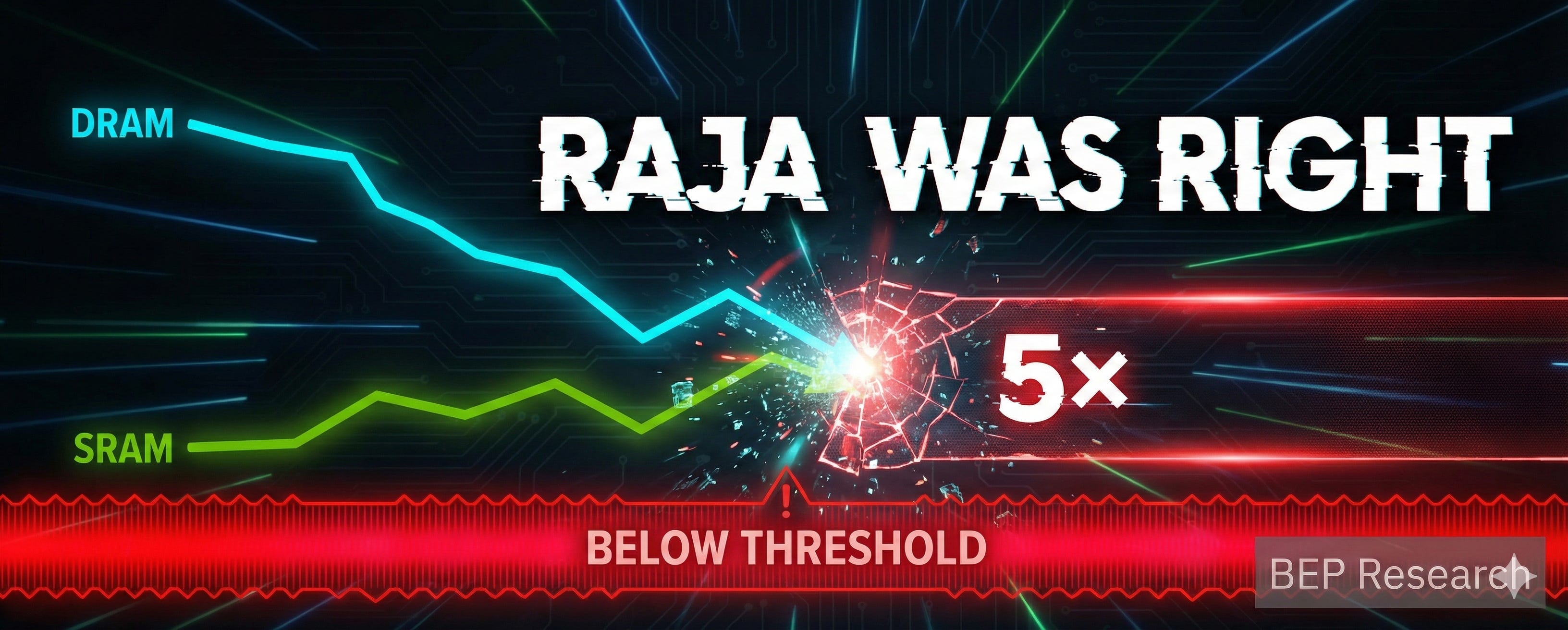
Raja Was Right
Part 1 of 3: The Memory Cost Reckoning

This is a new three-part series on the memory cost dynamics reshaping AI infrastructure. It builds directly on the themes from the Co-Design Series—where we explored The Memory Wall, NVIDIA’s Inference Stack Depth, and The Verification Gap. If you haven’t read those yet, start there. This series goes deeper into the economic forces behind the memory bottleneck.
In February 2024, Raja Koduri posted a warning that most people ignored.
The former Intel Chief Architect and AMD GPU lead—now on Tenstorrent’s board—laid out a simple thesis: if the DRAM/SRAM cost ratio drops below 5×, chip architects will switch to SRAM-based designs. And once they switch, the 3-4 year design cycle means it takes that long to switch back.
We crossed that threshold six months ago. The ratio is now approaching 2×.
This isn’t theoretical. It’s the economic foundation crumbling under Samsung, SK Hynix, and Micron’s $50+ billion annual HBM business. And it validates something I’ve been arguing throughout my research on AI infrastructure: the memory wall isn’t just a technical constraint. It’s reshaping competitive dynamics in ways that will echo for a decade.
The Original Warning
Raja’s February 17, 2024 post came with a chart showing LLM inference bandwidth versus capacity requirements. His observation was precise:
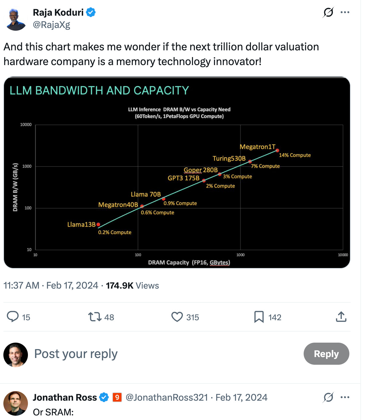
“If DRAM/SRAM $/byte ratio goes below 5x (due to irrational increase in DRAM pricing), most AI designs will be compelled to switch to SRAM and given the long design cycles, it will take 3-4 years to switch back, so if DRAM industry isn’t careful, it could lead to a crash in a couple of years.”
Jonathan Ross—Groq’s CEO—replied with a single word and a logo: “Or SRAM:” followed by the Groq emblem.
At the time, HBM3e traded at roughly 8× the cost of embedded SRAM per gigabyte. DDR5 server memory sat around 14×. The threshold seemed distant.
Then came Project Stargate. Then came the OpenAI-Microsoft infrastructure buildout. Then Samsung, SK Hynix, and Micron committed 35-40% of global DRAM wafer capacity to AI memory alone. DDR5 prices have more than tripled since September 2025. HBM3e supply remains structurally constrained through at least 2027.
The ratio collapsed.
The Numbers Today
Here’s where we stand as of Q1 2026:
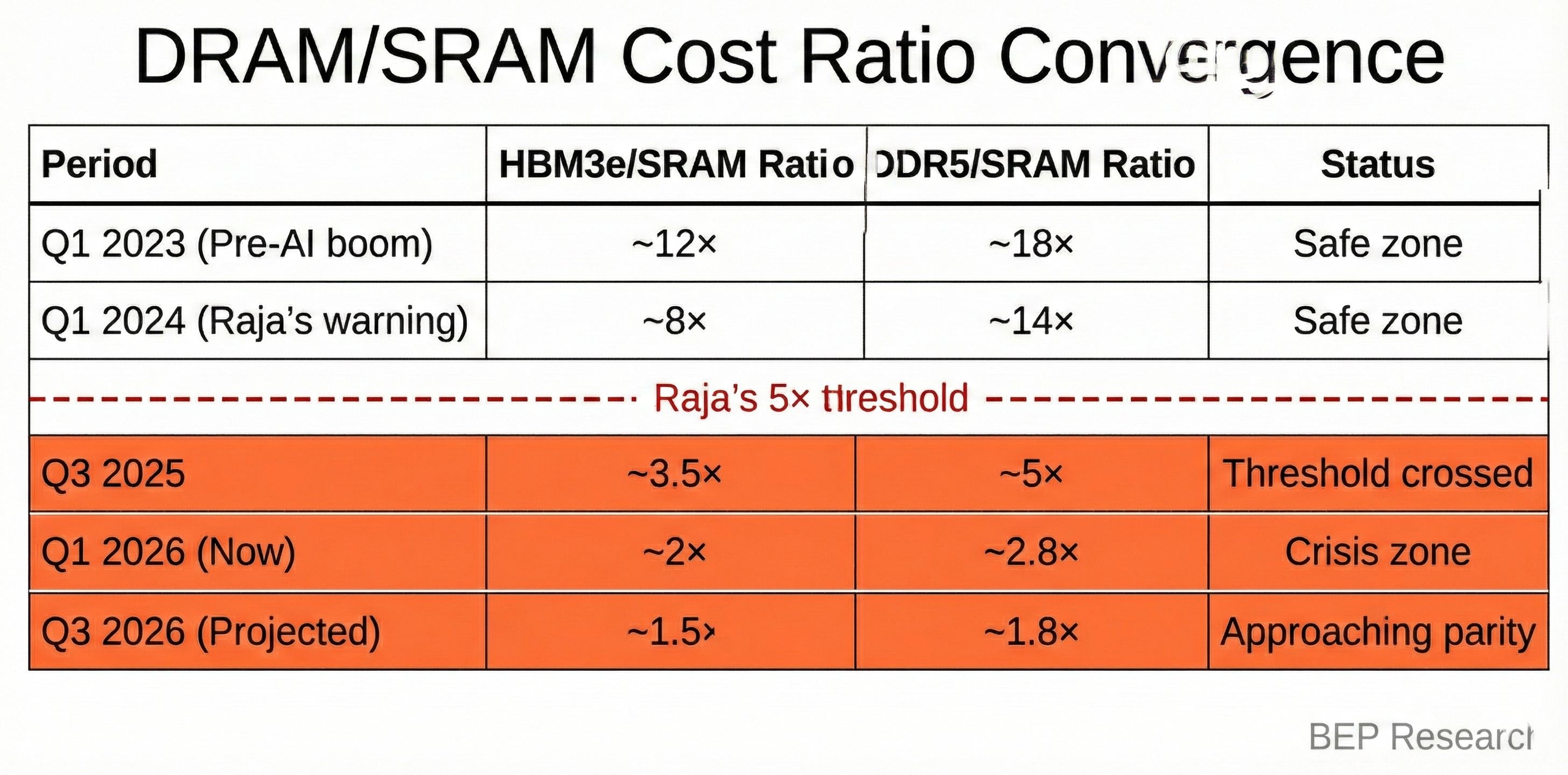
The SRAM cost estimates require some hedging. Semi Analysis puts on-chip SRAM at roughly 100× more expensive than commodity DRAM per bit—but that’s for dense, high-performance cache on leading-edge nodes. For specialized inference architectures like Groq’s LPU, which uses 230MB of SRAM on 14nm GlobalFoundries process, the economics are different. Industry estimates for production SRAM range from $40-100/GB depending on process node and volume.
The precise numbers matter less than the direction. Both ratios are compressing rapidly, and the structural drivers—AI-driven demand cannibalizing DDR5 production, new HBM fabs not coming online until 2028, SRAM costs declining on mature nodes—point toward continued convergence.
The 3-4 Year Ratchet Effect
Chip architectures aren’t switched like software deployments. The timeline from initial design to volume production spans 3-4 years minimum:
Year 1: Architecture definition, memory hierarchy decisions, IP licensing
Year 2: RTL design, verification, tape-out preparation
Year 3: Fabrication, packaging, bring-up, qualification
Year 4: Volume ramp, customer deployment
Architects making decisions right now for products shipping in 2029-2030 are staring at this convergence curve. If the ratio stays compressed—or continues falling—their entire economic model breaks.
The traditional calculus was simple: DRAM for capacity (cheap per bit, high density), SRAM for speed (expensive per bit, but 50-100× lower latency). Inference architectures split memory hierarchically, using HBM for model weights and on-chip SRAM for KV cache and intermediate activations.
But when DRAM costs approach SRAM costs, that hierarchy becomes a design constraint rather than an optimization. Why deal with HBM’s 100-150ns latency when you can get SRAM’s 0.5-2ns for nearly the same price?
This is what I call the ratchet effect: infrastructure buyers who committed to HBM-centric architectures in 2023-2024 are locked into those economics through 2027-2028. They can’t easily pivot to SRAM-heavy alternatives even if the cost curves favor them. But new designs—especially for edge inference where Raja sees the biggest disruption—face no such constraints.
The Grove Parallel: Industry Superstitions
Intel’s Andy Grove famously wrote about “superstitions” in corporate decision-making—the beliefs that persist long after the conditions that created them disappear. In Only the Paranoid Survive, he described how successful companies become prisoners of their past strategies.
I’ve thought about Grove a lot lately. The HBM superstition may be reaching its expiration date.
The superstition: AI inference requires HBM because training required HBM.
The reality: training and inference are fundamentally different workloads. Training processes data in massive parallel batches where memory bandwidth dominates. Inference decode is inherently sequential—one token at a time—where memory latency and capacity often matter more than raw bandwidth.
This distinction was at the heart of The Memory Wall—the first piece in my Co-Design Series. Groq’s entire architecture is built on this insight: trade HBM’s bandwidth for SRAM’s latency, and let deterministic execution hide the capacity limitations.
NVIDIA’s Hedge: The Groq Licensing Deal
NVIDIA isn’t waiting to find out who’s right. The ~$20 billion Groq licensing deal I covered in ‘Twas the Night Before Groq gives them optionality on both sides of the memory architecture question.
Groq’s LPU demonstrates what’s possible with SRAM-centric design: 230MB of on-chip memory per chip, no HBM, running on mature 14nm GlobalFoundries process. The architecture trades capacity for latency—and wins decisively on inference workloads where memory access patterns are predictable.
That’s not a limitation—it’s a template. As I noted in that piece:
“NVIDIA now has the IP to build a fast, inference-focused chip that sidesteps the two biggest capacity constraints in AI silicon: TSMC’s CoWoS packaging and the HBM supply chain dominated by SK Hynix and Samsung. Pair that with NVLink for chip-to-chip interconnect of LPU-style units, and you’ve got a scalable inference architecture that doesn’t compete for the same constrained resources as training GPUs.”
Intel’s Wild Card: The eDRAM Redemption Arc
The DRAM/SRAM cost convergence isn’t just about DRAM prices rising. SRAM economics may be improving faster than most analysts realize—and Intel sits at the center of this opportunity.
Alex_Intel_ , writing on Substack last week, laid out a compelling case. Intel has 1.83 million square feet of EUV-capable cleanroom space—plus additional non-EUV capacity—sitting underutilized. That’s optionality the market isn’t pricing.
His key insight on SRAM costs:
“SRAM haters are overestimating the cost. The SemiAnalysis model has Groq paying $5k per 14nm wafer. GlobalFoundries’ 14nm HD SRAM array density is roughly 10 Mbit/mm². Intel’s 18A HD SRAM is 38 Mbit/mm², and Intel might charge $20k to $25k per wafer for 18A. So you aren’t actually paying more per transistor compared to 14nm.”
The math matters: Intel’s 18A process achieves nearly 4× the SRAM density of GlobalFoundries’ 14nm. Even at higher wafer prices, the cost per bit is comparable—and the performance is significantly better. Higher density means higher bandwidth, and 18A’s improved gate control enables faster clock speeds.
But the real wild card is eDRAM—embedded DRAM that Intel pioneered at 22nm, placing capacitors in the metal stack to create pseudo-DRAM that’s 3-4× denser than SRAM while maintaining on-chip integration.
Raja himself weighed in on this recently:
“The eDRAM roadmap was very compelling going to 3nm and below...they even had a GPU taped-out and back using the 16/22nm version.”
If eDRAM scales as expected, a max reticle die could hold 12-16GB instead of 4GB—approaching Groq-tier capacity on a single chip. TSMC is reportedly working on similar technology now.
The investment implication: Intel isn’t just a foundry turnaround story. It’s potentially a beneficiary of the very memory cost convergence that threatens Samsung, SK Hynix, and Micron’s HBM business. The same cleanroom overcapacity that looks like a liability today could become a strategic asset if architects shift toward SRAM-heavy designs.
The Memory Industry’s Dilemma
Samsung, SK Hynix, and Micron face an existential strategic question.
On one hand, HBM pricing power has never been stronger. TSMC’s CEO confirmed CoWoS supply remains tight through 2026, HBM3e ASPs are seeing 20% price increases for 2026 contracts, and memory vendors are posting record margins.
On the other hand, those same elevated prices are accelerating the very dynamic Raja warned about. Every dollar of HBM pricing power today is a dollar of incentive for chip architects to design around DRAM dependency tomorrow.
The memory vendors’ rational response? Keep raising prices while demand is inelastic, use the profits to fund capacity expansion, and hope the new fabs come online before architects complete the switch to SRAM-heavy designs.
The timing is brutal. Micron’s Hiroshima HBM facility—announced with $9.6 billion in investment—won’t produce wafers until 2028. Samsung’s Pyeongtaek expansion prioritizes HBM and enterprise DRAM through 2027. SK Hynix’s advanced packaging lines are at capacity through 2026.
That’s a 2-3 year gap where supply remains constrained, prices stay elevated, and architects have every incentive to explore alternatives.
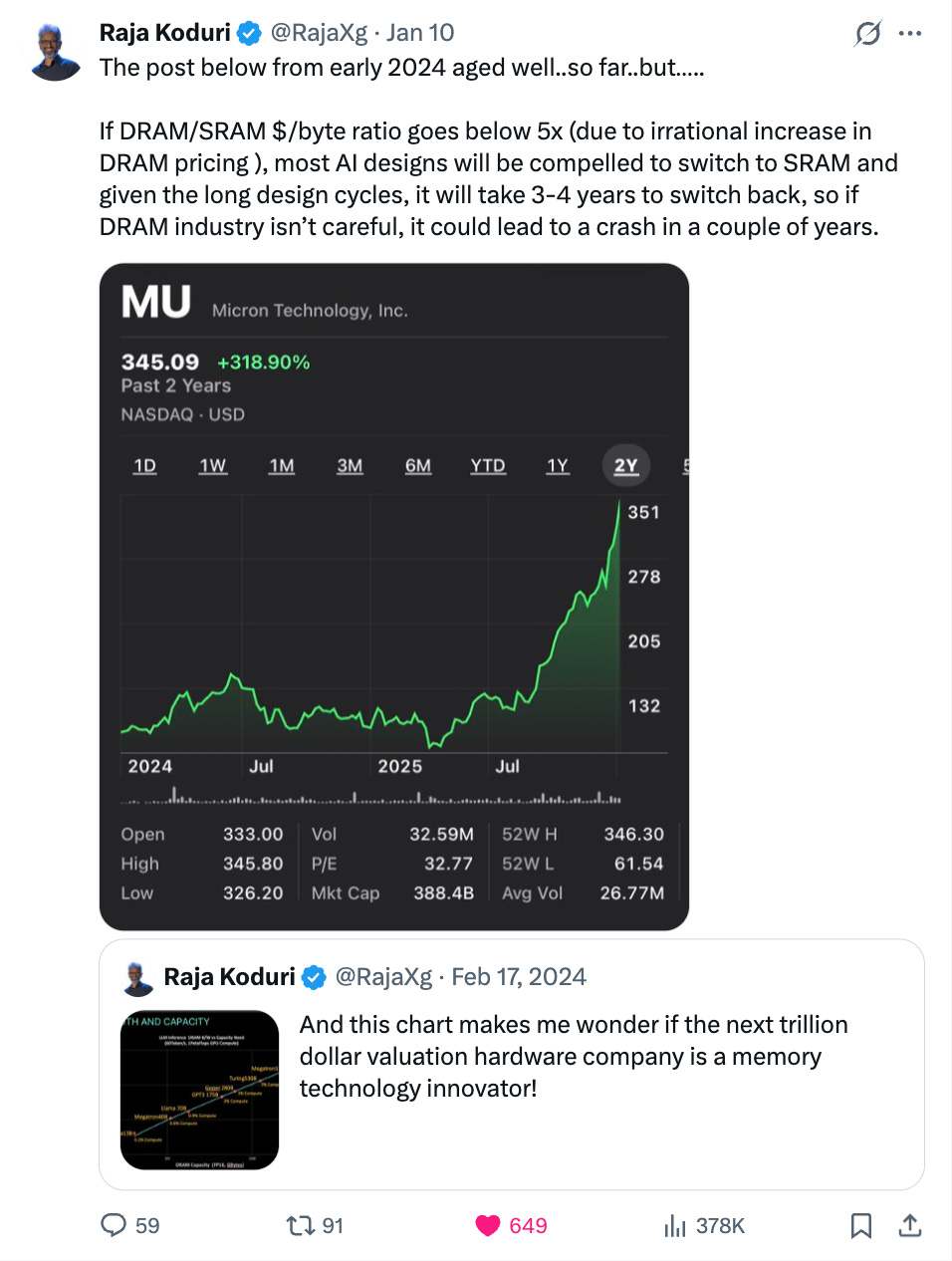
Raja’s Update
Earlier this month, Raja posted a follow-up on X:
“The post below from early 2024 aged well..so far..but.....”
That trailing ellipsis is doing a lot of work. Raja sees what I see: the threshold has been crossed, but the full consequences haven’t materialized yet. Chip architects are making decisions now that won’t ship products until 2029-2030. The DRAM industry has a narrow window to either normalize pricing or watch their market structurally shrink.
The “but” suggests Raja expects something to change. Either memory pricing corrects, new capacity arrives faster than expected, or some technological shift alters the economics.
Or the crash he predicted arrives on schedule, three years from now, when the designs being locked in today reach production.
Investment Implications by Time Horizon
Near-Term (2026-2027)
For NVIDIA investors: The Groq licensing deal and Feynman roadmap suggest NVIDIA recognizes the cost convergence threat and is building optionality. Their ability to mix HBM and stacked SRAM in future architectures provides a hedge regardless of how the ratio evolves.
For memory investors: The current earnings strength is real but potentially temporary. SK Hynix at ~62% HBM share looks dominant today, but the fundamental question is whether that share exists in three years.
Medium-Term (2027-2028)
For AMD investors: MI400 with up to 432GB HBM4 is impressive on paper, but AMD lacks NVIDIA’s hedge. They’re betting entirely on the HBM roadmap without the Groq IP, without the stacked SRAM capabilities, and with a software stack that still trails CUDA.
For Intel investors: The eDRAM and SRAM density advantages become relevant if architects shift. Watch for any foundry customer wins in inference-focused designs.
Long-Term (2028+)
For infrastructure investors: The companies supplying both paths—TSMC’s CoWoS for HBM integration AND hybrid bonding for 3D SRAM stacking—are positioned for either scenario. Applied Materials and Lam Research’s equipment serves both architectures.
What I’m Watching
Q2 2026: Memory vendor earnings commentary on HBM contract pricing for 2027. Any softening signals architects are hedging.
GTC 2026: NVIDIA’s inference roadmap updates. Specifically any mention of SRAM integration or architectural alternatives to pure HBM scaling.
TSMC’s CoWoS capacity announcements: The faster advanced packaging expands, the more pressure on HBM pricing to normalize.
Groq’s roadmap: As an independent entity under NVIDIA’s licensing umbrella, what architectural iterations emerge?
Coming Next Week
Part 2: The Hierarchy Rewrites — David Patterson’s January 2026 paper doesn’t just diagnose the memory problem—it prescribes four architectural directions that could reshape the competitive landscape. We’ll map each research direction to specific investment opportunities: High Bandwidth Flash, Processing-Near-Memory, 3D stacking, and low-latency interconnect. Plus Rick Xie’s controller-managed ECC thesis that could bend the HBM cost curve.
Part 3: The DRAM Squeeze — The deep dive you’ve been waiting for. We’ll examine how AI infrastructure is crowding out consumer electronics, validating the memory wall thesis in real-time. Smartphones are the first casualty—they won’t be the last. I’ll make the case for Rambus as the picks-and-shovels play on memory infrastructure, regardless of commodity price swings.
Subscribe to make sure you don’t miss them.
If you found this analysis valuable, please share it—it helps more than you know. And if you haven’t subscribed yet, now’s the time. BEP Research will be moving to paid soon. I’m committed to delivering institutional-quality analysis on AI infrastructure that you won’t find anywhere else.
Resources
Related BEP Research
The Memory Wall: Why Groq and Jamba Had to Find Each Other (Co-Design Series Part 1)
NVIDIA’s Inference Stack Depth Strategy (Co-Design Series Part 2)
The Verification Gap: Who Audits the Agent Swarm? (Co-Design Series Part 3)
‘Twas the Night Before Groq: NVIDIA’s Surprise Licensing Deal
The Packaging Paradox: Why CoWoS—Not 2nm—Is the Real AI Bottleneck
The Memory Wars: Why NVIDIA’s 2028 Architecture Ends the AI Chip Competition
About the Author
Ben Pouladian is a Los Angeles-based tech investor and entrepreneur focused on AI infrastructure, semiconductors, and the power systems enabling the next generation of compute. He was co-founder of Deco Lighting (2005–2019), where he helped build one of the leading commercial LED lighting manufacturers in North America. Ben holds an electrical engineering degree from UC San Diego, where he worked in Professor Fainman’s ultrafast nanoscale optics lab on silicon photonics and micro-ring resonators, and interned at Cymer, the company that manufactures the EUV light sources for ASML’s lithography systems.
He currently serves as Chairman of the Leadership Board at Terasaki Institute for Biomedical Innovation and is a YPO member. His investment research focuses on AI datacenter infrastructure, GPU computing, and the semiconductor supply chain. Long-term NVIDIA investor since 2016.
Follow on Twitter/X: @benitoz | More at benpouladian.com
Disclosure: The author holds positions in NVIDIA and related semiconductor investments. This is not investment advice.
Brilliant framing of the ratchet effect here. The timing really is brutal for memory vendors, they're locked into capacity expansions that wont deliver until 2028 while architects are making design decisions right now. I worked adjacent to semiconductor supply chain and the 3-4 year design cycle creates this weird lag where the market fundamentals have already shifted but nobody can pivot. The memory industry basicaly painted themselves into a corner with HBM pricing.
Hi Ben, thank you for your insightful articles. Please enable the Audio Play feature so we can listen instead of having to read each article. I always listen to articles on Substack, instead of reading, but, without the Play button, that simple action is harder. Thank you. 🙏