

The Bandwidth Tax
The real cost of HBM is levied on the system, not the stack.


Co-authored with Rui “Rick” Xie, researcher in computer systems, memory architecture, and AI infrastructure (rickxie.cn). Rick led the engineering and standards analysis; Ben Pouladian led the investment framing.
Irrational Analysis published “HBM: High-Bandwidth Mistake” on May 31, and it has been making the rounds ever since. The spicy takes, verbatim:
“I believe HBM is a mistake and will be phased out (90% drop in volume from peak) within the next 7-10 years.”
“DRAM stocks prob have another double or triple left in them.”
“At some point in the next 3-10 years, DRAM stocks will drawdown at least 70% from peak.”
The same week those lines were making the rounds, SK Hynix was booking the other side of the argument: its roughly $28 billion Nasdaq ADR offering, the second-largest US listing by a foreign company since Alibaba, came more than seven times oversubscribed ahead of Friday’s debut under SKHY. The loudest memory bear note of the summer and the most heavily bid memory listing in history landed in the same tape.
The volume-collapse call is the loud half of that note, and it is the half we think least matters to a portfolio. The quiet half is the one that reprices the memory complex: long before anyone phases HBM out, the money being made around each HBM stack starts growing faster than the money made inside it. We went looking for that line in the standards documents and the vendor disclosures. This piece is what we found, including the place where the data corrected our own first draft.
Everyone Is Long Memory on Scarcity. That Call Looks Right, for Now.
Start with what the bear note gets right, because it gets a lot right. Every major HBM vendor is effectively sold out. NVIDIA’s HBM4 bandwidth demand makes qualified stacks the binding constraint into 2027, and greenfield DRAM supply does not arrive in size before 2027-2028. Scarcity keeps pricing power with Micron, SK Hynix, and Samsung. Even the bear gives the equities “another double or triple” before the reckoning. We are not shorting memory into a sold-out tape, and neither is the author of the bear note.
But scarcity and value capture are different questions. One asks who is sold out today. The other asks who collects the incremental dollar as the system gets re-architected around the constraint. Those answers are already diverging, and the divergence is visible in public documents that most of the people sharing the bear note have not read.
Rick read them.
What the Standards Actually Say
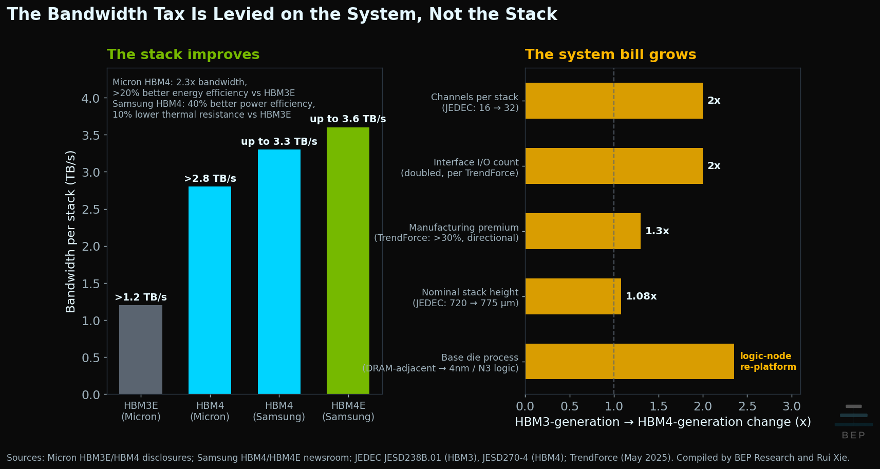
Our working draft of this piece assumed what most bandwidth-tax arguments assume: that each HBM generation delivers bandwidth at worsening cost and power per bit, and that the curve inside the stack is bending the wrong way. Rick went to the JEDEC standards and the vendor disclosures to anchor that chart, and came back with the correction that reshaped the piece: the public data do not show a worsening energy or cost curve per unit of delivered bandwidth. The stack is improving.
The numbers, from the vendors’ own disclosures:
Micron’s HBM3E delivers more than 1.2 TB/s per stack at pin speeds above 9.2 Gbps.
Micron’s HBM4 delivers more than 2.8 TB/s at above 11 Gbps: 2.3x the bandwidth of its HBM3E with over 20% better energy efficiency.
Samsung’s HBM4 reaches up to 3.3 TB/s at up to 13 Gbps, with reported 40% better power efficiency, 10% lower thermal resistance, and 30% better heat dissipation versus its HBM3E.
Samsung’s HBM4E samples run a stable 14 Gbps, scalable to 16, at up to 3.6 TB/s, with 16% better energy efficiency than HBM4.
A note on measurement boundaries: published pJ/bit figures often measure different parts of the memory path. Samsung’s 2023 HBM3 interface work reported 0.29 pJ/bit, while Intel’s 2025 HBM3 host-PHY paper reported 0.5 pJ/bit. Neither figure represents complete stack-access energy, and the two should not be combined into a cross-generation product series. The publicly available peer-reviewed data do not support a clean, apples-to-apples HBM3E-to-HBM4 stack-level pJ/bit chart. We wanted to build that chart. We couldn’t, so we didn’t.
So where is the tax? It moved. The bandwidth tax is levied at the system level: everything the platform must pay around the stack to turn a faster cube into delivered bandwidth. HBM4 doubles the channel count from 16 to 32 and doubles the interface width. Feeding that interface pulls the base of the stack onto advanced logic: Samsung builds its HBM4 base die on a 4nm logic node, and TSMC offers N12 and N3 processes for HBM4 base dies. JEDEC raised the nominal stack height from 720 to 775 microns and formally blessed 16-high configurations, which is more vertical room and also more layers, more parasitics, and more heat to manage within the defined HBM package envelope. TrendForce expects the manufacturing complexity to support a price premium above 30% for HBM4, driven by the doubled I/O count, larger die area, and the logic base die. Package area, power delivery, cooling, yield, qualification, and constrained packaging capacity all scale up alongside. That bill lands on the system, and it grows every generation even while the stack itself gets more efficient.
Hybrid bonding fits the same pattern, and this is Rick’s framing worth keeping: hybrid bonding is not a cost cure, it is an extension whose value rises as more layers, more channels, denser interconnects, and tighter thermal budgets have to fit inside that 775-micron envelope. Samsung reports hybrid copper bonding supports 16 or more layers while cutting thermal resistance by more than 20% versus thermal compression bonding. The instinct is familiar to BEP readers. As I wrote in The Memory Wars: “NVIDIA Feynman (2028) won’t fight SRAM physics. It routes around them: 3D-stacked SRAM using AMD X3D-style hybrid bonding.” Memory vendors are now doing to HBM what NVIDIA is doing to SRAM: routing around a wall rather than pushing through it, and paying for the route in packaging complexity.
The Migration Map
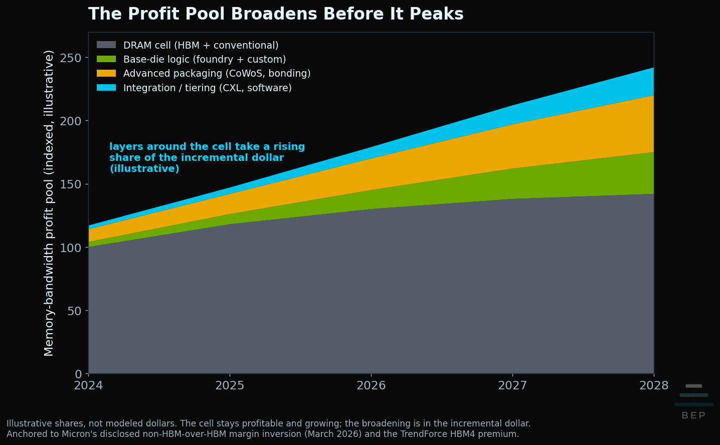
The claim we will defend is sharper than the one we started with. The consensus bull case says HBM stays scarce and the oligopoly keeps the margin. The circulating bear case says HBM gets phased out and the DRAM equities eventually round-trip. Rick’s read of the data supports a third path: the profit pool broadens before HBM volume or pricing ever peaks. HBM can remain scarce and highly profitable while foundries, base-die logic providers, packaging suppliers, and system integrators capture a rising share of each incremental bandwidth dollar. “Peak HBM” is in here somewhere as a pricing-power moment, but the broadening comes first.
There is already a first signature of it in Micron’s disclosed numbers. As I wrote in Micron Just Proved the Memory Thesis: “Sanjay confirmed that non-HBM margins are currently higher than HBM margins. That inverts the popular narrative that HBM is where all the pricing power lives.” One quarter of relative-margin commentary is a data point, not proof of a structural relocation. But when a top-three HBM vendor tells you its richest margins sit elsewhere in its stack, that is the tape’s first reading in the direction of the broadening.
Not every candidate destination is real. Rick placed each layer; the monetization read is mine.
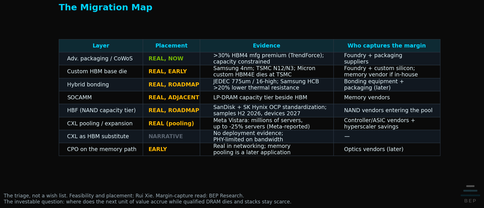
Three rows deserve words the table cannot hold. The packaging row is the argument from The Packaging Paradox: “the real bottleneck isn’t transistor density anymore. It’s advanced packaging.” The 30%-plus HBM4 manufacturing premium is that bottleneck showing up in a memory price. And the CXL row got materially stronger on June 29, when Meta disclosed Vistara, a custom CXL memory-expansion ASIC that reuses DDR4 from decommissioned servers as a slower capacity tier. Meta reports deployment across millions of production servers and up to a 25% reduction in server count for disaggregated ML inference. That is a hyperscaler saving real money with tiered memory in production, and it stays inside CXL’s actual lane: none of that DDR4 is doing HBM’s job.
The third row is the newest. SanDisk and SK Hynix began standardizing HBF this February: NAND stacked in an HBM4-matching footprint and power envelope, roughly 1.6 TB/s of read bandwidth per stack at 8 to 16 times the capacity of comparable HBM, with samples targeted for this half and the first inference devices in 2027. It is a capacity tier, not an HBM substitute, and demand forecasts cluster around 2030. The reason it earns a row now is who is building it: a flash vendor buying into the bandwidth profit pool is the broadening thesis in its purest form.
Rick’s one-line summary of the map is the line to keep: the investable question is where the next unit of value accrues while qualified DRAM dies and stacks remain scarce.
The Base Die Is the Cleanest Signal
Both JEDEC standards allow an optional logic die at the bottom of the stack for signal redistribution and vendor-defined functions. For most of HBM’s life that die was the memory vendor’s own, on a DRAM-adjacent process, and nobody outside the packaging team thought about it. That is over. Samsung’s HBM4 base die is built on its 4nm logic node. TSMC offers N12 and N3 base-die processes to the industry. Micron plans both standard and customized HBM4E base logic dies fabbed at TSMC, and has told investors it expects the customized products to carry higher gross margins.
Read that last disclosure the way we do: a memory vendor telling you that the customized logic at the bottom of the cube is where its own margin expansion lives. The margin is migrating inside the incumbent’s own product line, from the DRAM cell it has always sold to the logic and integration it is learning to sell.
Rick’s discipline on this point is worth quoting directly, because it is the part the custom-HBM hype skips: the base die does not add supply. It does not fix the shortage of DRAM core dies, known-good-die yield, stacking capacity, or packaging throughput. What it does is raise the system value of each scarce stack: interface optimization, offloaded host-die overhead, support logic pulled into the cube. Marvell claims its custom HBM architecture can cut memory-interface power by up to 70%, free up to 25% of compute-die area, and support 33% more memory capacity. Those are vendor architecture targets, not industry-measured results, and we label them as such. But the direction of every one of those numbers points the same way: the value of a stack increasingly depends on logic and packaging work done by someone other than a DRAM fab.
The Optical Off-Ramp Is Real. It Is Also Not Next.
The bear note’s proposed endgame is memory disaggregation over co-packaged optics: “HBM is a mistake. The solution is to disaggregate memory with a real PHY that drives co-packaged optics.” And a widely shared PhotonCap piece argued that the Micron-Anthropic HBM agreement accelerates that future, right in the headline: “The More Anthropic Buys Micron HBM, the Faster Optical Memory Pooling Arrives.”
Keep the claim narrow, because the sources themselves do. PhotonCap’s own body text concedes the deal “does not pull optical revenue forward so much as it strengthens the case for why optics becomes necessary,” and keeps optical memory revenue in FY2028 and beyond, with electrical CXL pooling entering revenue first. That matches Rick’s sequencing exactly, so we will state it as the joint view: CXL-based capacity pooling near term, optical scale-up interconnect next, optical memory pooling later. Optics improves reach and bandwidth density. A deployable memory system also needs end-to-end latency, coherence, data placement, reliability, yield, and customer qualification, and none of those ship on a press release. Marvell identifies all-optical scale-up interconnect as Celestial AI’s first commercial application. Optical memory pooling is also part of the platform vision, but its deployment timing is less clearly defined.
The same lesson is arriving from the latency side. A widely shared thread from the anonymous chip account Big Boss walked the interconnect math on sharded inference this week: hundreds of nanoseconds of SerDes and switch overhead, then tens of microseconds of software, wrapped around payloads measured in kilobytes. Whatever you make of his conclusions, the overhead math cuts our way: remote memory is only as useful as the fabric and placement layer serving it.
HBM scarcity strengthens the case for disaggregation. It does not, by itself, move the optical timeline. Both halves of that sentence matter, and most takes this month kept only one.
Three Ways We Are Wrong
1. Scarcity outruns the migration. If qualified HBM supply stays tight through 2028, the oligopoly’s pricing power persists and the broadening stays small relative to the cell’s profits. This is the strongest bear on our timing. Note what it does not touch: the direction. Even in this world, base-die value and the packaging premium grow; they just grow in the incumbents’ shadow for longer.
2. The destinations slip. CXL beyond the hyperscaler in-house case, SOCAMM volume, and custom base-die design-ins all carry integration friction. Meta building Vistara for itself is not the same thing as a merchant CXL market. If the “early” rows stay early, the incremental dollar has nowhere to migrate and defaults back to the cell.
3. The incumbents capture the migration internally. Micron fabbing custom base dies at TSMC and keeping the margin uplift is exactly this scenario, and Micron itself is telling you it plans to do it. If SK Hynix, Samsung, and Micron own the base die, the packaging relationships, and the customization revenue, the profit pool broadens but the tickers that own it barely change. Hold onto that nuance: a reader can accept our entire thesis and still be correctly long Micron. The difference is what you are long: the customization and integration line, not the commodity cell cycle.
What would change our mind. We are wrong on direction, not just timing, if two things happen together: the HBM base die stays overwhelmingly memory-vendor internal logic with no foundry co-design design-ins by late 2027, and Micron’s non-HBM margin leadership reverses for two or more consecutive prints. That is the clean disconfirming test, and we will run it in public.
So What?
Stop arguing about whether HBM disappears. On the published data, HBM is getting better per stack, per watt, and per delivered terabyte-per-second, and it is sold out. The question that reprices the complex is different: the system bill around each stack is growing every generation, and a growing share of that bill can accrue beyond the DRAM fabs. Foundries offering advanced-node base-die processes, including TSMC’s N12 and N3 options. HBM4 carrying an expected 30%-plus premium associated with higher manufacturing complexity. A hyperscaler cutting up to a quarter of its inference servers with a memory-tiering ASIC it designed itself.
For a decade, long memory meant long the DRAM cell. The bandwidth tax says the durable version of the trade is one level up: long the constraint, which is qualified bandwidth delivered into a rack, and long whoever gets paid to relieve it. Sometimes that is still the memory vendor; Micron’s custom base-die margins are the incumbents’ counterattack. Sometimes it is the foundry, the packager, or the CXL controller. The tells are concrete and they are all watchable this year.
And one ungated takeaway, so the free read carries a position and not just a concept: the layer already collecting the tax is advanced packaging, where TSMC and the packaging suppliers are pricing scarcity today, and the layer to underwrite next is the base die, where the foundry-plus-custom-silicon axis meets the memory vendors’ customization push. The under-covered names at both layers are the paid piece. The layers themselves you now have for free.
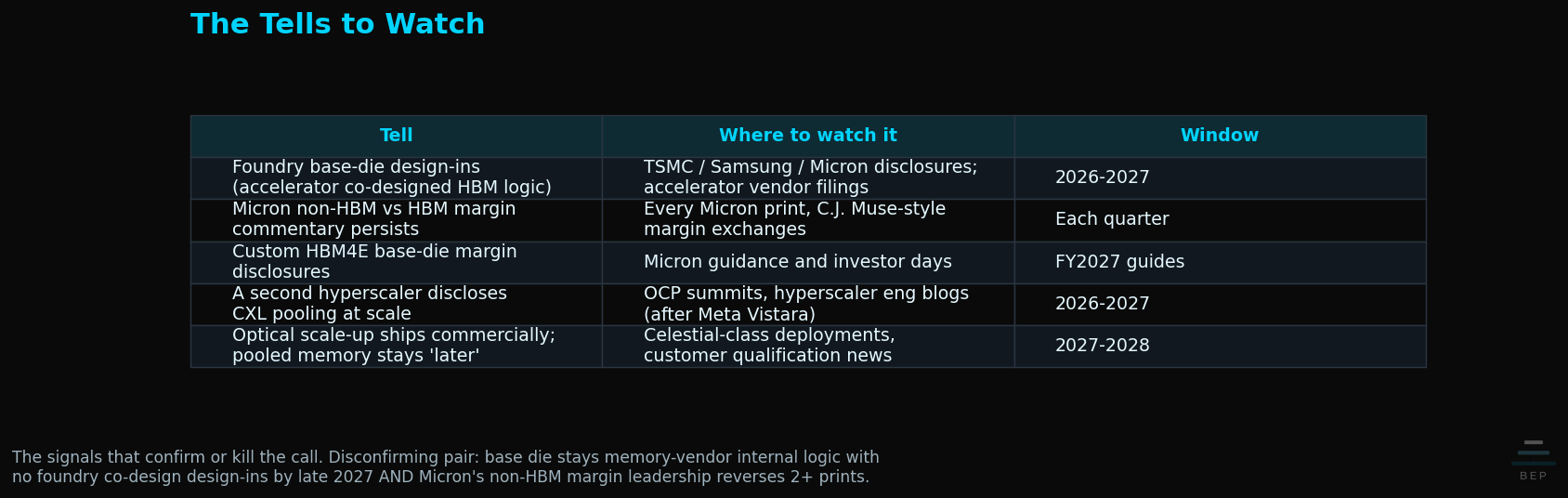
This reframe is free and citable on purpose; the thesis is the marketing. The paid follow-up, “The Bandwidth Tax: The Migration Call,” carries the trade: the entry framework for the pricing-power question, the under-covered base-die and OSAT names positioned for the broadening, position sizing, and the full watchlist with tickers. Rick and I will also do a joint Q&A in the Substack chat the day it drops, walking the engineering feasibility and the monetization read side by side.
Long the constraint, not the cell.
Sources
Irrational Analysis, HBM: High-Bandwidth Mistake (May 31, 2026)
Bloomberg on the SK Hynix US ADR offering (7x+ oversubscribed) (July 8, 2026)
Micron HBM3E product page; Micron HBM4 volume production release
Samsung commercial HBM4; Samsung HBM4E samples; Samsung hybrid copper bonding (GTC 2026)
JEDEC JESD238B.01 (HBM3) and JESD270-4 (HBM4), stack height and channel-count specifications
TSMC North America Technology Symposium release — N12 and N3 logic base die for HBM4
K. Chae et al., ISSCC 2023 (HBM3 interface, 0.29 pJ/bit); A. H. Mehta et al., VLSID 2025 (HBM3 host PHY, 0.5 pJ/bit) — interface/PHY boundary measurements
The Register on Meta’s Vistara CXL ASIC (June 29, 2026)
PhotonCap, The More Anthropic Buys Micron HBM, the Faster Optical Memory Pooling Arrives
Big Boss (@0xBADB01E), thread on interconnect overhead in sharded inference (July 5, 2026)
SanDisk and SK Hynix on HBF global standardization (Feb 25, 2026); TrendForce on HBF demand timeline
Related BEP Research
The Memory Wars: Why NVIDIA’s 2028 Architecture Ends the AI Chip Competition
The Packaging Paradox: Why CoWoS, Not 2nm, Is the Real AI Bottleneck
About the Authors
Rui “Rick” Xie is a researcher in computer systems, memory architecture, and AI infrastructure (rickxie.cn). For this piece he went to the JEDEC HBM3 and HBM4 standards and the primary vendor disclosures directly, built the feasibility triage in the migration map, and corrected the piece’s original framing when the data disagreed with it. That correction is the piece. His views and analysis are his own and do not represent his employer.
Ben Pouladian is the publisher of BEP Research and CEO of BEP Holdings. He led the investment framing and the margin-capture analysis. Framings are credited to their originators throughout. More at www.bepresearch.com
Disclosure: The author holds positions in NVDA, LITE, CRDO, TSEM, ALAB, LSCC, WOLF, ORCL (2027 LEAPS), and BE as disclosed in prior pieces. This is investment research, not investment advice. Do your own work.
 | A guest post by
|