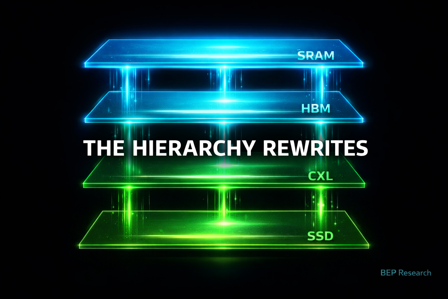
The Hierarchy Rewrites
Part 2 of 3: The Memory Cost Reckoning

This is Part 2 of the Memory Cost Reckoning series. Part 1: Raja Was Right established the crisis—the DRAM/SRAM cost ratio collapsed from 12× to 2× in three years, crossing the threshold Raja Koduri warned about in 2024. Today, we examine the industry’s response. If you haven’t read Part 1 yet, start there.
Last week’s analysis established the crisis: Raja Koduri’s 5× cost threshold warning has materialized. The DRAM/SRAM ratio collapsed from 12× to 2× in three years. Chip architects making decisions today for 2029-2030 products are staring at economics that break their traditional memory hierarchy assumptions.
Today, we examine the response.
David Patterson’s January 2026 paper doesn’t just diagnose the problem—it prescribes four architectural directions that could reshape the competitive landscape. This carries the Turing Award laureate’s imprimatur: Patterson co-developed RISC, created RAID, and wrote the textbook that trained a generation of chip architects. When he says “the primary challenges are memory and interconnect rather than compute,” the industry listens.
Let’s unpack what this means for investors.
The Patterson Paper: A Turing Laureate’s Stamp
Patterson’s paper with Xiaoyu Ma from Google DeepMind makes a stark claim that reframes how we should evaluate AI infrastructure:
“The autoregressive Decode phase of the underlying Transformer model makes LLM inference fundamentally different from training. Exacerbated by recent AI trends, the primary challenges are memory and interconnect rather than compute.”
This isn’t a critique of NVIDIA or HBM suppliers. It’s a diagnosis that the entire industry optimized for the wrong bottleneck. Training needed compute density and memory bandwidth. Inference decode needs memory capacity, latency, and interconnect efficiency.
The paper identifies four research directions. Each creates investment themes:
1. High Bandwidth Flash (HBF): 10× memory capacity with HBM-like bandwidth for inference workloads
2. Processing-Near-Memory (PNM): Logic integrated with memory to reduce data movement
3. 3D Memory-Logic Stacking: Vertical integration of compute and memory dies
4. Low-Latency Interconnect: Network topologies optimized for inference’s small, frequent messages
Patterson explicitly notes that the current philosophy of “full-reticle die with high FLOPS, many HBM stacks, and bandwidth-optimized interconnect” is a mismatch to LLM decode inference. The companies that recognize this—and build accordingly—capture the next wave of value.
This echoes what I argued in The Memory Wall—the first piece in my Co-Design Series. The memory wall isn’t just a constraint; it’s reshaping which architectural approaches win.
Rick’s REACH Thesis: Bending the HBM Cost Curve
Before declaring HBM dead, consider how it might evolve.
Memory architecture researchers including Rick Xie have articulated the REACH thesis: controller-managed ECC could bend the HBM cost curve by shifting error correction from the memory die to the controller. Current HBM implements ECC at the DRAM level, consuming die area and power for every memory stack.
The insight: for inference workloads with high temporal locality (the same weights accessed repeatedly), controller-level ECC can achieve equivalent reliability with less memory-side overhead. This could enable either cost reduction or capacity increase at the same price point.
SK Hynix and Samsung are reportedly evaluating these approaches for HBM4E variants. The implication: the HBM cost curve may have more room to flatten than current projections suggest—but only for specific workload profiles.
For investors, this creates a nuanced picture. HBM isn’t dead, but the assumption of linear cost scaling may be wrong in both directions—worse for capacity-bound workloads (where HBF wins), better for bandwidth-bound workloads (where ECC optimization helps).
The Tiered Architecture: Context is the New Bottleneck
Patterson’s paper and NVIDIA’s CES 2026 announcements converge on the same architectural insight: the future isn’t a single memory tier. It’s a hierarchy optimized for different access patterns
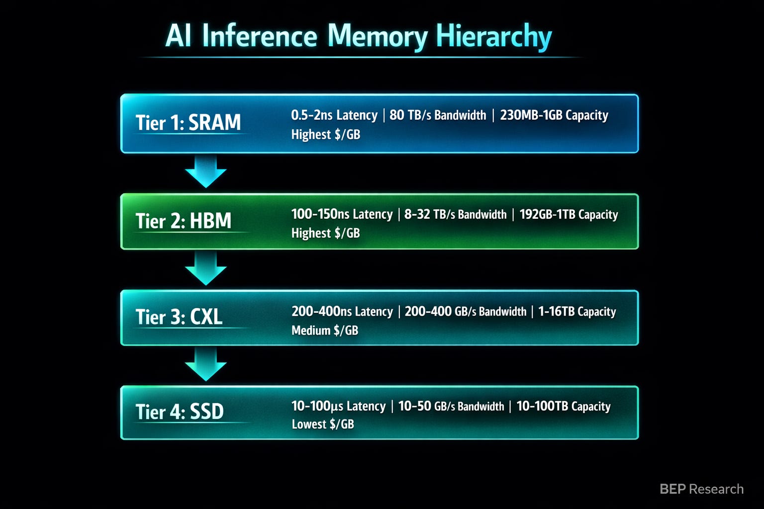
Jensen Huang crystallized this at CES: “Context is the New Bottleneck.” The memory hierarchy for AI inference now spans HBM → System Memory → Rack SSD → Network SSD. His exact words: “Storage must be rearchitected.”
NVIDIA’s response is the Context Memory Storage Platform: BlueField-4 DPUs managing KV cache lifecycle—deciding what stays in HBM, what gets pushed to NVMe, and what gets shared across the rack. The system delivers 5× higher tokens per second and 5× higher power efficiency for context-heavy workloads.
This is co-design in action—the theme I’ve been developing since The Verification Gap. The DPU, the NVMe controllers, the network fabric, and the GPU memory system all work together. You can’t buy this capability off the shelf—it requires coordinated design across silicon, firmware, and software.
The Runtime Layer: Where Memory Meets Workload
In conversations with inference optimization researchers—including insights from Prashanth at InferX—a pattern emerges: the runtime layer is where the memory hierarchy meets the workload.
The key insight: different inference patterns require different memory policies. A conversational chatbot with short context windows has different memory needs than a code assistant processing entire repositories. A real-time voice agent with sub-100ms latency requirements can’t tolerate the same memory tier transitions as a batch document processor.
What this means practically:
Hot Path Optimization: Frequently accessed model weights should live in SRAM or HBM. Runtime systems that predict access patterns can pre-stage data in faster tiers.
KV Cache Management: Long-context models (100K+ tokens) generate KV caches that exceed HBM capacity. Runtime policies that intelligently evict and reload from SSD tiers enable workloads that would otherwise be impossible.
Speculative Prefetch: If the runtime knows the next likely tokens (speculative decoding), it can pre-load relevant attention weights before they’re needed—hiding memory latency behind computation.
The companies building these runtime optimizations—whether as standalone products or integrated into inference stacks—capture value that chip vendors alone cannot.
Company-by-Company Investment Implications
NVIDIA: Stack Depth as Memory Moat
NVIDIA’s response to the memory wall isn’t better GPUs—it’s owning more of the stack. The $30 billion+ in acquisitions and licensing deals since 2024 maps directly to memory hierarchy layers:
Mellanox ($6.9B): Network fabric for distributed memory
Run:ai (~$700M): Orchestration that pools GPU memory across clusters
Deci (~$300M): Model optimization that reduces memory footprint
Groq licensing (~$20B): SRAM-centric architecture concepts
BlueField-4: DPU-managed tiered memory
This is the “stack depth” thesis I developed in NVIDIA’s Inference Stack Depth Strategy—Part 2 of the Co-Design Series. NVIDIA isn’t buying market share; they’re buying architectural optionality across every layer of the memory hierarchy.
AMD: All-In on HBM
AMD’s MI400 with up to 432GB HBM4 is impressive on paper—but it’s a single-path bet. They lack:
SRAM hedge: No Groq-equivalent licensing or internal SRAM-centric architecture development
Tiered memory stack: No BlueField equivalent for intelligent cache management
Software depth: ROCm still trails CUDA in ecosystem breadth
If the DRAM/SRAM ratio continues compressing, AMD’s entire roadmap is exposed. They’re betting the memory hierarchy assumptions of 2024 still hold in 2028.
Intel: The Packaging Wild Card
Intel’s EMIB (Embedded Multi-die Interconnect Bridge) and Foveros 3D stacking technologies represent something the market isn’t pricing: the ability to build memory-centric inference architectures that sidestep both CoWoS constraints and HBM supply chains entirely.
As I noted in Part 1: Raja Was Right, Intel’s 18A process achieves nearly 4× the SRAM density of GlobalFoundries’ 14nm. Combine that with their packaging portfolio, and Intel could become the foundry of choice for architects designing around the memory cost convergence.
The same excess capacity that looks like a liability on quarterly earnings calls becomes a strategic asset when architects need alternatives to the TSMC/SK Hynix duopoly.
Patterson’s Four Directions: Investment Mapping
Direction 1: High Bandwidth Flash (HBF)
Patterson’s paper highlights HBF as delivering “10× memory capacity with HBM-like bandwidth.” For inference workloads where capacity (holding the full model) matters more than raw bandwidth, this changes the economics entirely.
Beneficiaries: Sandisk/Western Digital (direct), NAND flash equipment suppliers (Applied Materials, Lam Research, Tokyo Electron), companies building HBF-optimized inference engines.
Direction 2: Processing-Near-Memory
PNM integrates logic with memory to reduce data movement. Patterson notes it’s better suited for LLM inference than processing-in-memory (PIM) because shards can be 1,000× larger.
Beneficiaries: Samsung (already shipping PIM products), startups like Upmem, memory companies with fab capacity for custom logic integration.
Direction 3: 3D Memory-Logic Stacking
Vertical integration of compute and memory dies through hybrid bonding. This is NVIDIA’s Feynman approach—stack SRAM on cheaper nodes, bond to compute on leading-edge nodes.
Beneficiaries: TSMC (SoIC technology), Intel (Foveros), AMD (extending 3D V-Cache to AI), hybrid bonding equipment suppliers (Besi, EVG, SUSS).
Direction 4: Low-Latency Interconnect
Patterson argues current interconnects optimized for training’s large batch transfers are mismatched to inference’s small, frequent messages. New topologies (dragonfly, high-dimensional tori) and processing-in-network could help.
Beneficiaries: Astera Labs (CXL/PCIe), Marvell (custom silicon), companies building processing-in-network solutions, potentially NVIDIA’s Spectrum-X if they pivot toward latency optimization.
The Synthesis: Specialization, Not Death
Patterson and Raja aren’t predicting HBM’s death. They’re describing its specialization.
The memory hierarchy that served training—where HBM bandwidth justified premium pricing—fragments for inference. Different workloads, different optimal architectures, different cost curves:
Training and Prefill: HBM remains essential. Bandwidth-bound, parallel processing, established supply chain.
Large-Model Decode: Tiered hierarchy wins. HBM for hot weights, CXL for warm data, SSD for cold context.
Edge Inference: SRAM-centric architectures compete. Lower latency, simpler supply chain, cost convergence makes economics work.
Capacity-Bound Workloads: HBF could dominate. 8× capacity advantage for long-context models, RAG systems, persistent memory.
For investors, this creates both opportunity and risk:
Opportunity: Companies building for the tiered memory world—whether NVIDIA’s integrated stack or specialized solutions at each layer—capture value that commodity chip suppliers cannot.
Risk: Companies whose investment thesis assumes HBM pricing power continues across all workloads may face multiple compression as the market fragments.
The Patterson paper provides the intellectual framework. Raja’s cost ratio data provides the economic catalyst. The market will provide the verdict.
What I’m Watching
HBF Standardization Progress: The Sandisk/SK Hynix collaboration determines whether HBF becomes a real product or vaporware.
Intel 18A Customer Wins: Any inference-focused design wins signal the SRAM density thesis is gaining traction.
Memory Vendor Earnings: Commentary on 2027 HBM contract pricing reveals whether architects are hedging.
NVIDIA’s Inference Roadmap: GTC 2026 should reveal how seriously they’re pursuing SRAM-heavy alternatives alongside HBM.
Coming Next Week: The Deep Dive
Part 3: The DRAM Squeeze — This is the deep dive you’ve been waiting for. We’ll examine how AI infrastructure is crowding out consumer electronics in real-time, validating everything we’ve discussed in Parts 1 and 2.
The evidence is stark: smartphone OEMs are being forced to choose between 30% price increases or spec downgrades. Qualcomm is considering 5-10% price cuts to support customers squeezed by memory costs. The “more specs for less money” model that defined consumer electronics for fifteen years is breaking.
I’ll make the investment case for Rambus as the picks-and-shovels play—benefiting from memory volume regardless of commodity price swings. Controller-managed ECC, DDR5 interface dominance, and MRDIMM chipsets position them at the exact chokepoint where value accrues.
The memory wall isn’t abstract anymore. It’s reshaping entire industries. Next week, we see it in action.
Subscribe to make sure you don’t miss it.
If you found this analysis valuable, please share it—it helps more than you know. And if you haven’t subscribed yet, now’s the time. BEP Research will be moving to paid soon. I’m committed to delivering institutional-quality analysis on AI infrastructure that you won’t find anywhere else.
Resources
SDxCentral: “AI inference crisis: Google engineers on why network latency and memory trump compute”
Semiconductor Engineering: “Four Architectural Opportunities for LLM Inference Hardware”
This Series: The Memory Cost Reckoning
Part 1: Raja Was Right — The 5× threshold and the economics reshaping chip architecture
Part 2: The Hierarchy Rewrites — Patterson’s roadmap and who wins (you are here)
Part 3: The DRAM Squeeze — The deep dive on consumer casualties and the Rambus thesis (coming next week)
Related BEP Research
The Memory Wall: Why Groq and Jamba Had to Find Each Other (Co-Design Series Part 1)
NVIDIA’s Inference Stack Depth Strategy (Co-Design Series Part 2)
The Verification Gap: Who Audits the Agent Swarm? (Co-Design Series Part 3)
NVIDIA CES 2026: Six Chips, One Platform, and the Extreme Codesign Era
The Packaging Paradox: Why CoWoS—Not 2nm—Is the Real AI Bottleneck
The Memory Wars: Why NVIDIA’s 2028 Architecture Ends the AI Chip Competition
About the Author
Ben Pouladian is a Los Angeles-based tech investor and entrepreneur focused on AI infrastructure, semiconductors, and the power systems enabling the next generation of compute. He was co-founder of Deco Lighting (2005–2019), where he helped build one of the leading commercial LED lighting manufacturers in North America. Ben holds an electrical engineering degree from UC San Diego, where he worked in Professor Fainman’s ultrafast nanoscale optics lab on silicon photonics and micro-ring resonators, and interned at Cymer, the company that manufactures the EUV light sources for ASML’s lithography systems.
He currently serves as Chairman of the Leadership Board at Terasaki Institute for Biomedical Innovation and is a YPO member. His investment research focuses on AI datacenter infrastructure, GPU computing, and the semiconductor supply chain. Long-term NVIDIA investor since 2016.
Follow on Twitter/X: @benitoz | More at benpouladian.com
Disclosure: The author holds positions in NVIDIA and related semiconductor investments. This is not investment advice.
Couldn't agree more. The emphasis on memory and interconnect for LLM inference realy changes how I see future AI infrastructure. What do you think this means for practical, scalable deployment? Brilliant post.