

The Shoreline Problem: A Bear Case on HBM
HBM did not solve memory bandwidth. It worked around it. The real bottleneck was never the memory, it is the chip edge. The bear case on HBM, and why I still would not bet against NVIDIA


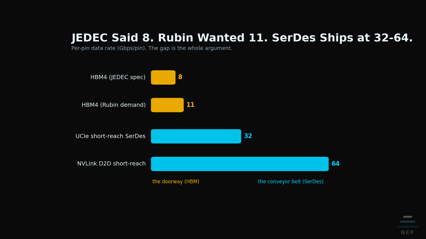
JEDEC Said 8. Rubin Demanded 11. All Three Vendors Struggled.
Here is the line in the spec sheet almost nobody is reading. JEDEC, the body that standardizes memory, rated HBM4 at 8 gigabits per pin. NVIDIA’s Rubin asked for 11. A 38% reach, and SK Hynix, Samsung, and Micron all strained to hit it. Read that next to the fact that short-reach SerDes links, the ones already shipping in UCIe and NVLink die-to-die today, run at 32 to 64 gigabits per pin. Four to eight times faster. On the same silicon, in the same datacenter, in the same year.
That gap is the whole argument. The semiconductor analyst Irrational Analysis made it in a piece called “HBM: High Bandwidth Mistake,” and it stopped me cold this afternoon. So I had to think about this and break down his claim, stated simply: the problem was never the DRAM. The DRAM is fine. The problem is how we bolted it on. What follows is my attempt to translate his engineering argument for the rest of us, and to connect it to a piece of physics I have already written about from the other side of the stack.
The Chip Is a Kitchen. Memory Is the Pantry.
Think of the chip as a kitchen full of cooks, and memory as the pantry of ingredients. The cooks are fast. The question is always the same: how fast can ingredients reach them.
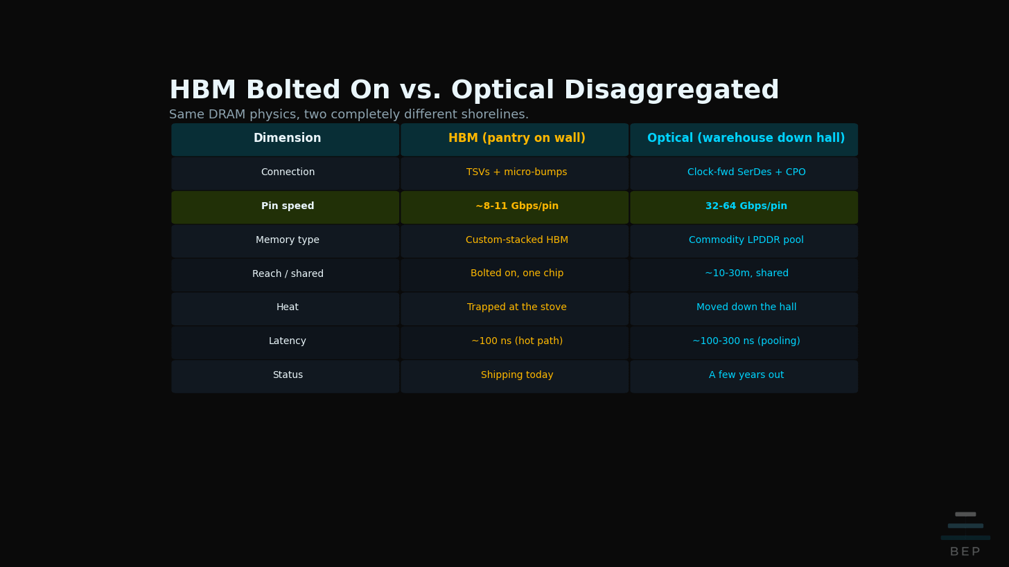
Today, with HBM, the only way to get ingredients fast enough is to bolt the pantry directly onto the kitchen wall, stacked floor to ceiling. It works. But the shelves are crammed together with thick support beams running through them. Those beams are the TSVs and micro-bumps, the through-silicon vias and the tiny solder contacts that stitch the stacked memory dies together. Each one adds a little electrical drag, what an engineer calls parasitic capacitance, and that drag is what caps how fast each pin can run. The beams also eat shelf space and make the pantry door narrow. So no matter how fast the cooks are, ingredients come through at a trickle.
And the pantry is stuck. You cannot move it. You cannot share it with the kitchen next door. All that stacked mass traps heat right next to the stove, so the cooks have to slow down to keep from cooking themselves. That is HBM in one image: a powerful pantry strangled by its own doorway.
The reframe is that simple. Memory bandwidth has been treated as a memory problem. It is really a shoreline problem: the doorway writ large. How much usable edge does the chip have, and how efficiently can data cross it? The DRAM was never the bottleneck. The doorway was.
His Fix: Rip the Pantry Off the Wall, Pipe It In From Down the Hall
So stop bolting the pantry to the wall. Put it down the hall, and connect it with a fiber-optic conveyor belt instead of a doorway.
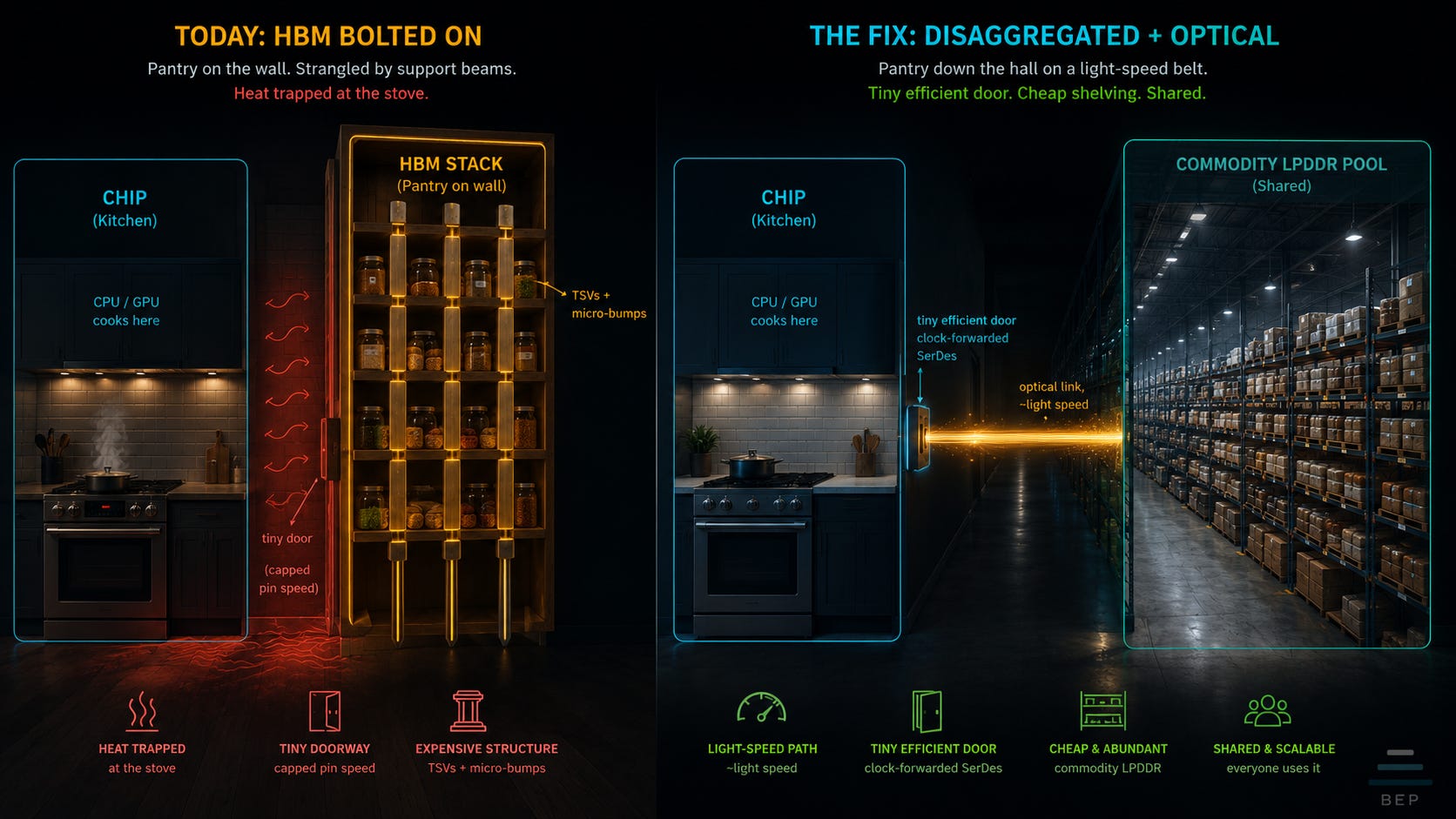
The belt moves ingredients at near light speed with almost no delay. The door on the kitchen side is now tiny and efficient, a clock-forwarded SerDes feeding a simple receiver, which frees up wall space for more cooks. The pantry can be cheap, ordinary shelving, commodity LPDDR instead of expensive custom-stacked HBM. Any kitchen can draw from the same pantry. You can make it as big as you want. And with the heat moved down the hall, the stove can finally run hotter.
He is honest about the catch, and so am I. Building the conveyor belt is hard. Getting the data onto the fiber cleanly is, in his words, pain and suffering, and it is a few years out. Until then the smart move is a better-organized wall pantry, which is the commodity-LPDDR approach he likes from a startup called Positron.
I Already Wrote the Other Half of This Story
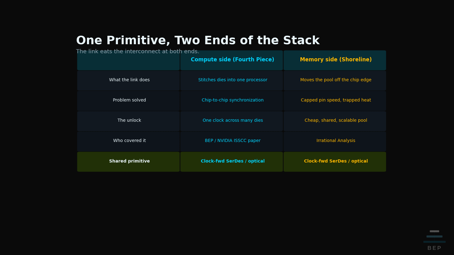
Here is the connection only this newsletter can make. The “clock-forwarded SerDes” at the heart of his fix is not a new idea to BEP readers. It is the exact same primitive I traced from NVIDIA’s ISSCC paper earlier this year.
As I wrote in The Fourth Piece: Why Groq Changes the GTC Thesis: “Optical clock forwarding lets NVIDIA connect multiple separate chips so they behave as one coherent processor. Same clock, same timing, every cycle.” In that piece, I read clock forwarding as the way NVIDIA makes separate dies act as one machine at rack scale, the physical layer that lets a dataflow inference engine stay synchronized. Same enabling technology. Opposite end of the stack. I covered it for unifying compute. Irrational Analysis applies it to disaggregating memory.
These are not competing theses. They are two consequences of the same physics. A forwarded clock over an optical link is so precise it can make two chips share one heartbeat, and that single capability eats the interconnect at both ends. On the compute side, it stitches dies into one coherent processor. On the memory side, it lets the pantry move down the hall. The piece of silicon doing the real work in both stories is the link, not the chip and not the DRAM.
The Bear Case: “Almost No Delay” Is Doing Heavy Lifting
I want to be honest about where the metaphor stretches, because two words in his pitch carry a lot of weight: “almost no delay.”
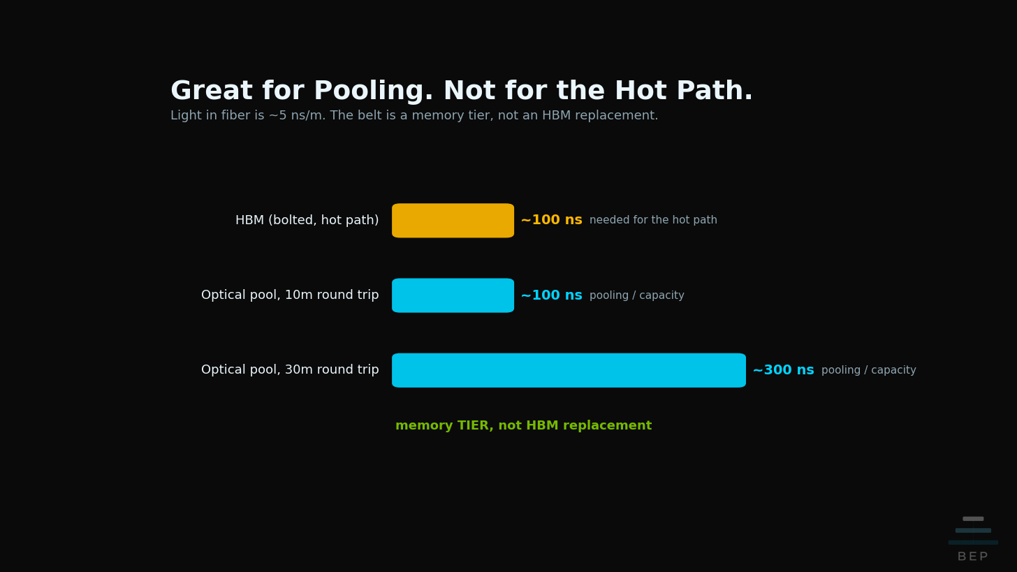
Light in fiber travels at roughly 5 nanoseconds per meter. A pantry 30 meters down the hall is a 60-meter round trip, so call it 300 nanoseconds of pure flight time before you touch anything. HBM bolted to the wall answers in roughly 100 nanoseconds. So the belt is wonderful for pooling capacity and bandwidth, the bulk ingredients you can fetch a little ahead of time. It is not a drop-in replacement for the latency-sensitive hot path, the ingredients the cook needs in the next half-second.
That distinction softens his most aggressive claim, his projection that HBM volume drops 90%. The honest version is that the optical pool becomes a memory tier, a big cheap warehouse behind a smaller fast wall pantry, not a full HBM replacement. The physics on the shoreline is settled. The demand-destruction timing is the speculative part. Hybrid bonding, the next-generation way of stacking dies without the bulky micro-bumps, may let HBM widen its own doorway and reclaim some of the shoreline it is losing.
Here is the cleanest way the whole reframe could be right and still not pay. If the co-packaged optical receiver never gets cheap and reliable enough to beat HBM-plus-hybrid-bonding inside an investable window, the shoreline argument is true and commercially irrelevant for a decade. So watch the receiver, not the slogan. The day a co-packaged optical link ships at an HBM-competitive cost per bit is the day the pantry actually moves down the hall.
And the largest caveat sits above all of it: NVIDIA. The company leads the entire stack, sets the roadmap the memory vendors chase, and has a long habit of engineering its way out of its own constraints rather than being disrupted by them. Apple did the same thing with the iPhone supply chain, turning the hardest manufacturing problem in consumer electronics into a moat nobody else could cross. Whichever way the shoreline resolves, NVIDIA is positioned to own it. Widen HBM’s doorway with hybrid bonding, or pull the optical link in-house and make the disaggregated pantry its own. Betting on this kind of disruption usually means betting against the incumbent, and the incumbent here writes the spec. That is the discipline in the call: the physics points one way, but the company best placed to capture it is the same one that built the wall pantry. Until that resolves, the fight is only over how fast HBM fades.
So What?
Stop thinking about memory bandwidth as a memory problem. Start thinking about it as a real-estate problem at the edge of the chip. That is the reframe to carry out of this piece, and it reorganizes the whole stack once you see it. The expensive, supply-constrained, heat-trapped thing we have been treating as the prize, the HBM stack, turns out to be a workaround for a doorway that was always too narrow. The real prize is the doorway itself, the link that crosses the shoreline. That is the layer the market keeps pricing as a cost when it is actually the control point.
I am not calling the end of HBM. The fight is only over how fast it fades.
Watch the shoreline, and watch the link that crosses it.
Credit
This is a free, standalone read, and there is no paywalled second half. Full credit to Irrational Analysis for the original engineering argument in “HBM: High Bandwidth Mistake.” I am translating it and adding the bear case, not improving on his physics. I would rather hand you the caveat straight than sell you the clean version.
Related BEP Research
About the Author
Ben Pouladian is a Los Angeles-based tech investor and entrepreneur focused on AI infrastructure, semiconductors, and the power systems enabling the next generation of compute. He holds an electrical engineering degree from UC San Diego, where he worked in Professor Fainman’s ultrafast nanoscale optics lab on silicon photonics and micro-ring resonators, and interned at Cymer, the company that manufactures the EUV light sources for ASML’s lithography systems. Long-term NVIDIA investor since 2016.
Follow on X: @benitoz | More at bepresearch.com
Disclosure: The author holds positions in NVDA, BE, LITE, CRDO, TSEM, LSCC, ORCL 2027 Calls, and ALAB. This is not investment advice.
Disaggregated memory was a theme we explored 15 years ago when I ran a cloud infrastructure dev team at Microsoft Research. We even had a private meeting with Jenson to explore several opportunities including a disaggregated memory pool solution for GPU, CPU and FPGA hybrid designs. In the end, the opportunity never panned out for several reasons. Clearly the additional latency, especially with copper became a showstopper for latency sensitive workloads. And multi-master implications to queuing latency compounded the already problematic limitations of copper. Optical may help in this regard. But your article got me thinking tactically about MU as an investment.
On the most recent Micron earnings call, CEO Sanjay Mehrotra's confirmed that non-HBM margins currently exceed HBM margins. UBS quantified this, projecting traditional DRAM gross margins reaching 67% in Q2 2026 versus HBM's 62%, widening to 75% by Q4 2026. This inverts the popular narrative that HBM is where all pricing power lives. The reason is structural, not cyclical: every HBM4 wafer displaces approximately three conventional DRAM wafers while achieving lower yields (~50% HBM vs. ~70% for DDR5). By starving the conventional DRAM market to feed HBM, the memory industry has inadvertently made the product it's diverting away from more profitable than the premium product itself. Now lets layer on the implications of agentic AI...
I have yet to see a comprehensive analysis for how agentic CPU demand affects DRAM demand. With current GPU to CPU ratios of 4:1 to 8:1 evolving to 1:1 as agentic workloads flood into datacenters. For DRAM the implication appears structurally MORE positive — if HBM fades, the replacement architecture runs on commodity DRAM/LPDDR, which Micron produces at higher yields and currently at higher margins compared to complex HBM stacks. This is a net positive for MU provided agentic demand exceeds the marginal reduction of HBM disaggregation. But I suspect a massive shift away from HBM will reduce the DRAM premium as greater wafer supply floods into the DRAM market. This will be one to watch.
Thanks for another thought provoking article!
This is the picks-and-shovels thesis stated in a single layer, and it's the cleanest version I've read. Bandwidth was never a memory problem, it's a real-estate problem at the chip edge, which is exactly why I stopped trying to pick the winning accelerator and started owning the layers that get paid no matter which one wins. The link is the control point precisely because the market keeps pricing it as a cost.
The shoreline can resolve four ways: optical disaggregation, hybrid-bonding/3D-DRAM widening HBM's own doorway, wafer-scale integration that erases the edge (Cerebras), or compute-in-memory that never crosses it (d-Matrix). The architecture is the contested layer. But across all four branches the same three slices get paid: the interconnect that crosses the shoreline, the bulk DRAM bits in whatever form they take, and the power to run the hotter stove your last image promised. I'd rather own the layers than the kitchen.
Long the networking/optical complex and power, plus CBRS as the erase-the-edge bet. Also long d-Matrix. #NotAdvice