

Applied Materials Just Confirmed the Packaging Thesis
Earnings Flash: Record DRAM, GAA tooling launches, and a Q2 guide that says the equipment cycle is accelerating.


Applied Materials reported fiscal Q1 2026 results tonight, and the numbers tell a clear story: the AI equipment supercycle isn’t slowing down it’s shifting into the exact segments we’ve been tracking.
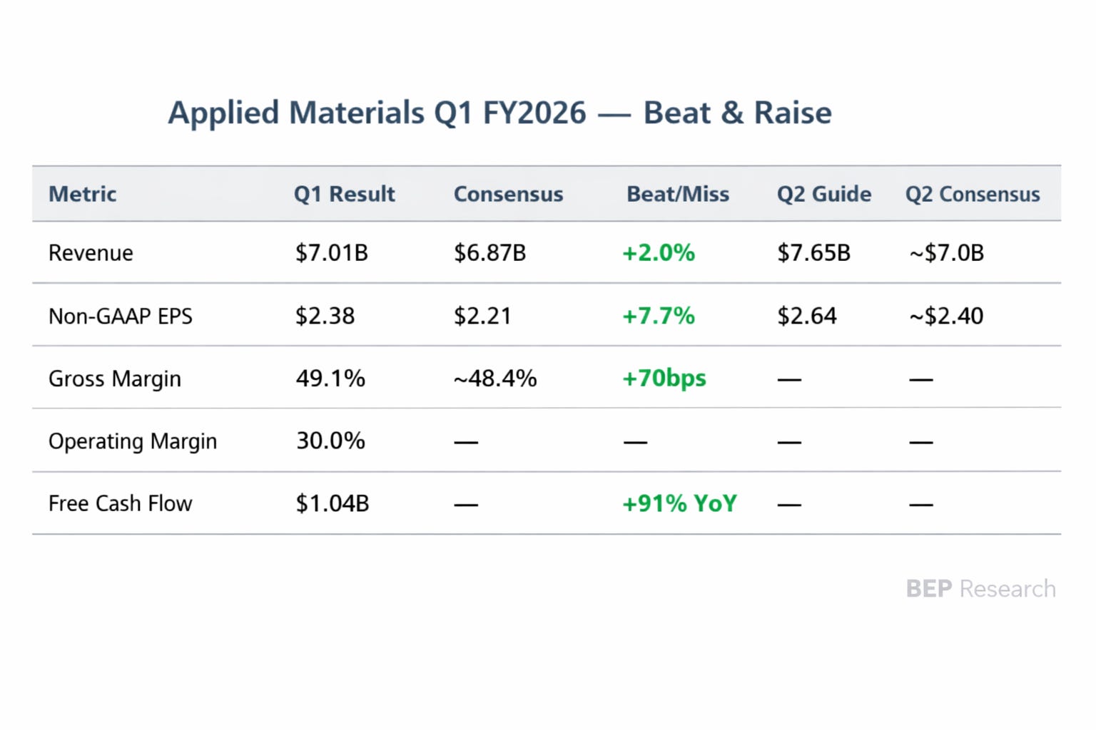
Revenue came in at $7.01 billion, beating the $6.87 billion consensus by 2%. Non-GAAP EPS of $2.38 crushed the $2.21 Street estimate by 7.7%. But the real signal isn’t the beat—it’s where the dollars are flowing and what management just guided for next quarter.
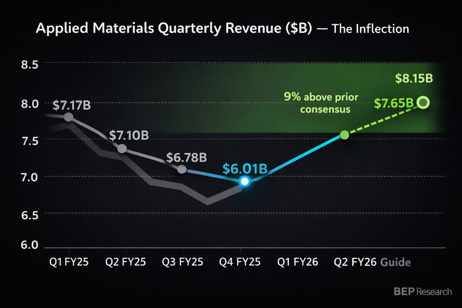
For context: Applied’s own Q1 guidance from November was $6.85 billion ± $500 million. They didn’t just hit the high end they blew past it. And then they guided Q2 to $7.65 billion at the midpoint, roughly 9% above where the Street was sitting heading into the print.
Three signals from this quarter connect directly to the thesis laid out in The Packaging Paradox and The Memory Wars.
Signal 1: Record DRAM Revenue Confirms the Memory Equipment Cycle
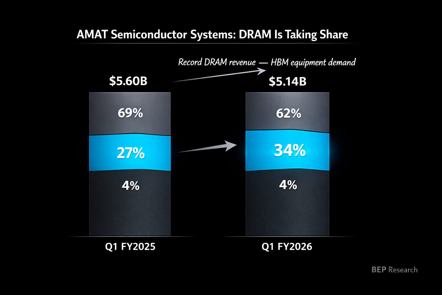
The most important line in the entire release: Semiconductor Systems achieved record DRAM revenue.
DRAM jumped from 27% to 34% of Semiconductor Systems revenue quarter-over-quarter. In dollar terms, that’s approximately $1.75 billion in DRAM equipment revenue versus roughly $1.51 billion a year ago—a 16% increase even as total Semiconductor Systems revenue declined 8% year-over-year (from $5.60 billion to $5.14 billion).
This isn’t legacy DRAM spending. This is HBM packaging equipment, advanced deposition for through-silicon vias, and the bonding and thinning tools required to stack 12 and eventually 16 layers of DRAM within JEDEC’s 775μm height limit. As I wrote in The Memory Wars, the 16-Hi HBM race requires wafers thinned to 30μm—silicon so thin it’s translucent—with bonding layers shrinking below 10μm. That level of precision requires new equipment from exactly the vendors reporting tonight.
On the call, management made the roadmap even more aggressive: DRAM stacking is moving from 12 to 16 to 20 layers. Each additional layer compounds the equipment intensity — more deposition steps, more thinning passes, more bonding cycles, more metrology checkpoints. If 12-Hi HBM3e already strains existing tool capacity, imagine the equipment demand when fabs are running 20-Hi stacks at volume. This is why Applied is doubling manufacturing capacity and still building inventory. The equipment content per HBM stack is on an exponential curve.
On the earnings call, management made the supply picture even more explicit: “Leading edge foundry logic and DRAM capacity is essentially full and prices have increased.” Full utilization plus pricing power is the exact combination that drives equipment upgrade cycles. When your customers’ fabs are running at capacity and they’re charging more per wafer, the return on new equipment investment accelerates—and so do orders.
The foundry/logic mix declined from 69% to 62%, which initially looks concerning. But the context matters: China restrictions have compressed the addressable logic market, while DRAM—specifically HBM and advanced DRAM for AI—is pulling forward capacity investment faster than anyone modeled three quarters ago. The mix shift is a feature, not a bug.
Signal 2: The GAA Tooling Wave Is Real
Applied launched three new systems this quarter, all targeting 2nm Gate-All-Around transistors and advanced wiring—the exact equipment intensity increase I quantified in The Packaging Paradox.
Viva is a pure radical treatment that smoothens GAA silicon nanosheets with atomic-level precision. Sym3 Z Magnum is a conductor etch system delivering angstrom-level 3D trench profile control. And Spectral is an atomic layer deposition system that replaces tungsten transistor contacts with molybdenum—a new contact metal that lowers resistance at the critical junction between transistors and copper wiring.
That last one deserves attention. The tungsten-to-molybdenum contact transition has been discussed in academic circles for years, but Applied just productized it. Lower contact resistance directly improves transistor switching speed and power efficiency at the 2nm node—and it requires entirely new deposition chemistry. Translation: this isn’t an upgrade to existing tools. It’s a new tool sale for every leading-edge fab.
In The Packaging Paradox, I noted that equipment revenue per 100,000 wafer starts per month expands from approximately $6 billion to $7 billion with GAA and backside power delivery. These product launches are how that $1 billion of incremental revenue per unit of capacity materializes in Applied’s order book.
Signal 3: The Q2 Guide Says the Acceleration Is Real
The forward guide is the most bullish signal in the release. Applied guided Q2 fiscal 2026 revenue to $7.65 billion ± $500 million, with non-GAAP EPS of $2.64 ± $0.20.
To put that in perspective: the Q2 revenue midpoint is 9% sequential growth and implies the highest quarterly revenue Applied has reported since Q1 FY2025. More importantly, it was well above where the Street was positioned—consensus for the April quarter had been sitting around $7.0 billion prior to this print.
CEO Gary Dickerson’s prepared remarks connected the dots explicitly: “The need for higher performance and more energy-efficient chips is driving high growth rates for leading-edge logic, high-bandwidth memory and advanced packaging. These are areas where Applied is the process equipment leader, and we expect to grow our semiconductor equipment business over 20 percent this calendar year.”
Twenty percent growth in semiconductor equipment. That’s not a vague aspiration—that’s a company with visibility into customer commitments through calendar 2026. When the process equipment leader for deposition, etch, and packaging tells you they expect 20%+ growth, they’re telling you their customers (TSMC, Samsung, SK Hynix, Micron) are placing orders for capacity that won’t come online for 12-18 months.
The call reinforced this with unusual specificity. Management noted they are “tracking higher levels of planned CapEx from cloud service providers” and that customers “are increasing the number of new factory projects and fab expansions scheduled to be completed over the next several years.” That’s not next-quarter demand—that’s multi-year visibility into facility build-outs that haven’t even broken ground yet.
Applied is betting with its own balance sheet, too. They’ve “proactively increased inventory by nearly $500 million year over year” to meet what they see coming, and have “nearly doubled system manufacturing capacity” over the past several years. Equipment companies don’t build inventory speculatively at this scale. They build it because customers have committed to taking delivery.
But the most striking comment came during Q&A. Dickerson described conversations with his largest customer CEOs and R&D leaders, calling AI datacenter demand “a significant wave that’s going to last over a longer period of time.” Customers are talking about “extremely high compound annual growth rates” — and then he dropped this: datacenter is on track to pass PCs and eventually smartphones in total wafer starts.
Let that sink in. Smartphones drove the last decade of semiconductor capacity investment. If datacenter wafer starts are approaching that scale, the equipment addressable market isn’t just growing it’s structurally re-rating upward. Dickerson added that based on customer conversations, he expects 2027 to also be “a very strong year.” This isn’t one quarter of momentum. It’s a multi-year cycle with visibility extending well beyond the current guide.
The Noise: BIS Settlement and China
The quarter included a $253 million legal settlement with the U.S. Commerce Department’s Bureau of Industry and Security over export controls compliance—a previously disclosed matter now resolved. This is a one-time charge that artificially depressed GAAP operating margin to 26.1% versus the cleaner non-GAAP 30.0%. The DOJ and SEC closed their investigations without action.
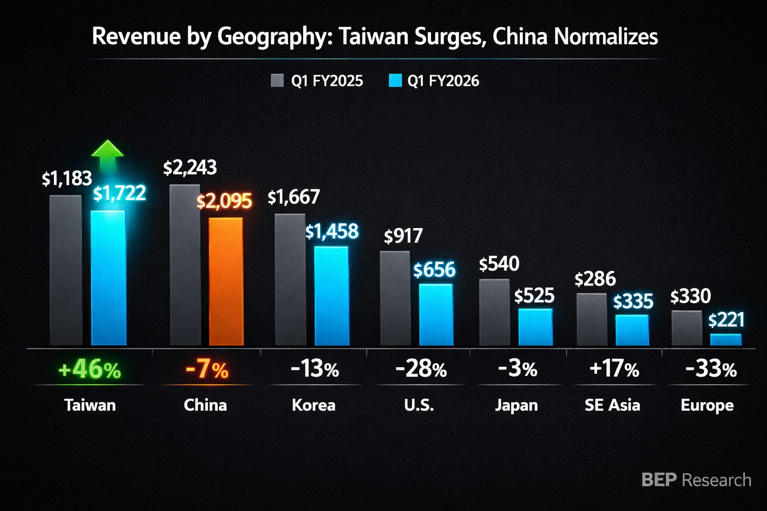
China revenue ticked down slightly from 31% to 30% of total revenue, or $2.10 billion. Still elevated relative to the long-term mix, but the trajectory is clearly downward from the 45% peak in early fiscal 2025. In The Packaging Paradox, I flagged China exposure as a key risk for equipment names, and the normalization is playing out as expected. Applied’s ability to grow the top line while China declines speaks to the strength of the AI-driven demand elsewhere—particularly Taiwan (up from 17% to 25% of revenue) and Korea (steady at 21%).
Applied Global Services: The Recurring Revenue Story
AGS delivered record revenue of $1.56 billion, up 15% year-over-year with operating margin expanding from 24.9% to 28.1%. The installed base of equipment keeps growing, and as fabs add more complex tools for GAA and advanced packaging, the services and spares revenue attached to those tools grows proportionally.
This segment doesn’t get the attention it deserves. AGS is a higher-margin, recurring revenue stream that provides downside protection through cyclical troughs. At a $6.2 billion annualized run rate, it’s becoming a meaningful contributor to total company profitability.
So What?
The equipment intensity thesis is playing out in real-time. GAA transistors, HBM packaging, and advanced wiring all require more equipment per wafer start than prior generations. Applied’s record DRAM revenue, new GAA product launches, and 20%+ growth outlook for calendar 2026 confirm that the capex cycle is accelerating, not plateauing.
The memory equipment cycle is the AI packaging cycle. Record DRAM revenue isn’t about commodity memory. It’s about the deposition, bonding, thinning, and metrology tools required to build HBM3e and HBM4 stacks at scale. Every HBM stack that ships inside an NVIDIA Blackwell or Vera Rubin module required equipment from companies like Applied Materials and Lam Research to manufacture.
The Q2 guide resets expectations for the group. If Applied is guiding $7.65 billion for April, Lam Research and KLA likely have similar tailwinds. Equipment investors should watch for read-through when those companies report.
China normalization is manageable. Applied grew the top line guidance while China revenue continued its decline from peak levels. The AI demand from Taiwan, Korea, and U.S.-based fab construction is more than offsetting export control headwinds.
The call confirmed multi-year visibility. Management isn’t just guiding one quarter ahead—they’re describing a multi-year cycle of new factory projects and fab expansions. Combined with proactively building $500 million in inventory and doubling manufacturing capacity, Applied is positioning for sustained demand, not a one-quarter spike. For investors in the equipment space, the message is clear: this cycle has legs.
This is a quick earnings reaction. For the full framework on why advanced packaging capacity—not transistor density—is the real AI bottleneck, see The Packaging Paradox. For the memory bandwidth thesis, see The Memory Wars.
What’s Changing at BEP Research
On March 9th, BEP Research is moving to paid subscriptions.
The timing is deliberate: NVIDIA’s GTC conference starts the following week, and I will be there in person. Paid subscribers will get exclusive access to real-time GTC coverage—in-depth analysis of every major announcement, on-the-ground interviews, and breakdowns of what the roadmap changes actually mean for your portfolio. Not recaps. Real analysis, in real time.
After March 9th, free subscribers will still receive post summaries and occasional public pieces. But the deep work—the Co-Design Thesis series, investment frameworks, earnings breakdowns, supply chain deep dives, and all GTC coverage—moves behind the paywall.
Pricing
Because you have been here from the beginning, I am offering an early bird rate that disappears when the paywall goes live:
Early Bird: ~$350/year (13% off) — available now through March 9th only.
→ Lock in the Early Bird rate here
After March 9th, standard pricing applies:
Annual: $400/year
Monthly: $45/month
Founding Member: $450/year — for those who want to go above and beyond in supporting BEP Research. Founding Members get permanent recognition as the people who backed this work from day one, and will get priority consideration as I build out the institutional tier.
I will be direct: this is premium-priced for a Substack. It is priced that way on purpose. I am building institutional-quality research without sell-side conflicts, without advertising, and without the surface-level takes that dominate financial media. If even one analysis helps you size a position correctly or avoid a bad trade, the subscription pays for itself many times over. Several of you have already told me exactly that.
About the Author
Ben Pouladian is a Los Angeles-based tech investor and entrepreneur focused on AI infrastructure, semiconductors, and the power systems enabling the next generation of compute. He was co-founder of Deco Lighting (2005–2019), where he helped build one of the leading commercial LED lighting manufacturers in North America. Ben holds an electrical engineering degree from UC San Diego, where he worked in Professor Fainman’s ultrafast nanoscale optics lab on silicon photonics and micro-ring resonators, and interned at Cymer, the company that manufactures the EUV light sources for ASML’s lithography systems.
He currently serves as Chairman of the Leadership Board at Terasaki Institute for Biomedical Innovation and is a YPO member. His investment research focuses on AI datacenter infrastructure, GPU computing, and the semiconductor supply chain. Long-term NVIDIA investor since 2016.
Follow on Twitter/X: @bepresearch | More at benpouladian.com
Disclosure: The author holds positions in NVIDIA and related semiconductor investments. The author may initiate positions in companies mentioned in this article. This is investment research, not advice. Do your own work.